
Substrate susceptor and deposition apparatus having same

Active Publication Date: 2013-05-16
KOOKJE ELECTRIC KOREA
View PDF4 Cites 22 Cited by
  • Summary
  • Abstract
  • Description
  • Claims
  • Application Information

AI Technical Summary

Benefits of technology

The patent invention improves the temperature distribution and efficiency of heating a substrate placed on a susceptor. This means that the substrate can be made smaller while still maintaining consistent temperature across the entire surface. Additionally, the process of heating the substrate may be more efficient, meaning it takes less time to achieve the desired temperature.

Problems solved by technology

However, according to the atomic layer deposition process, it takes a long time to grow a layer having a desired thickness because a deposition rate is very slow when compared to a chemical vapor deposition process or a sputtering process.
Thus, productivity may be decreased.
The susceptor may thermally affect the substrate according to a disposition shape of a heating element to cause non-uniformity of the layer.

Method used


Image

  • Substrate susceptor and deposition apparatus having same
  • Substrate susceptor and deposition apparatus having same
  • Substrate susceptor and deposition apparatus having same

Examples


embodiments

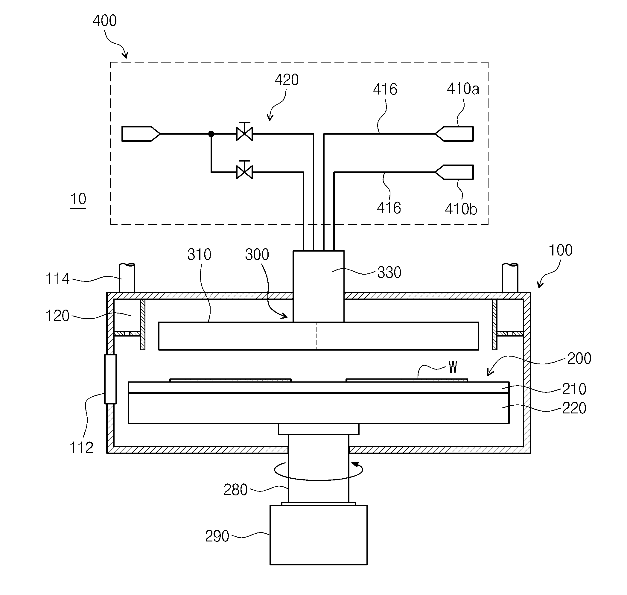
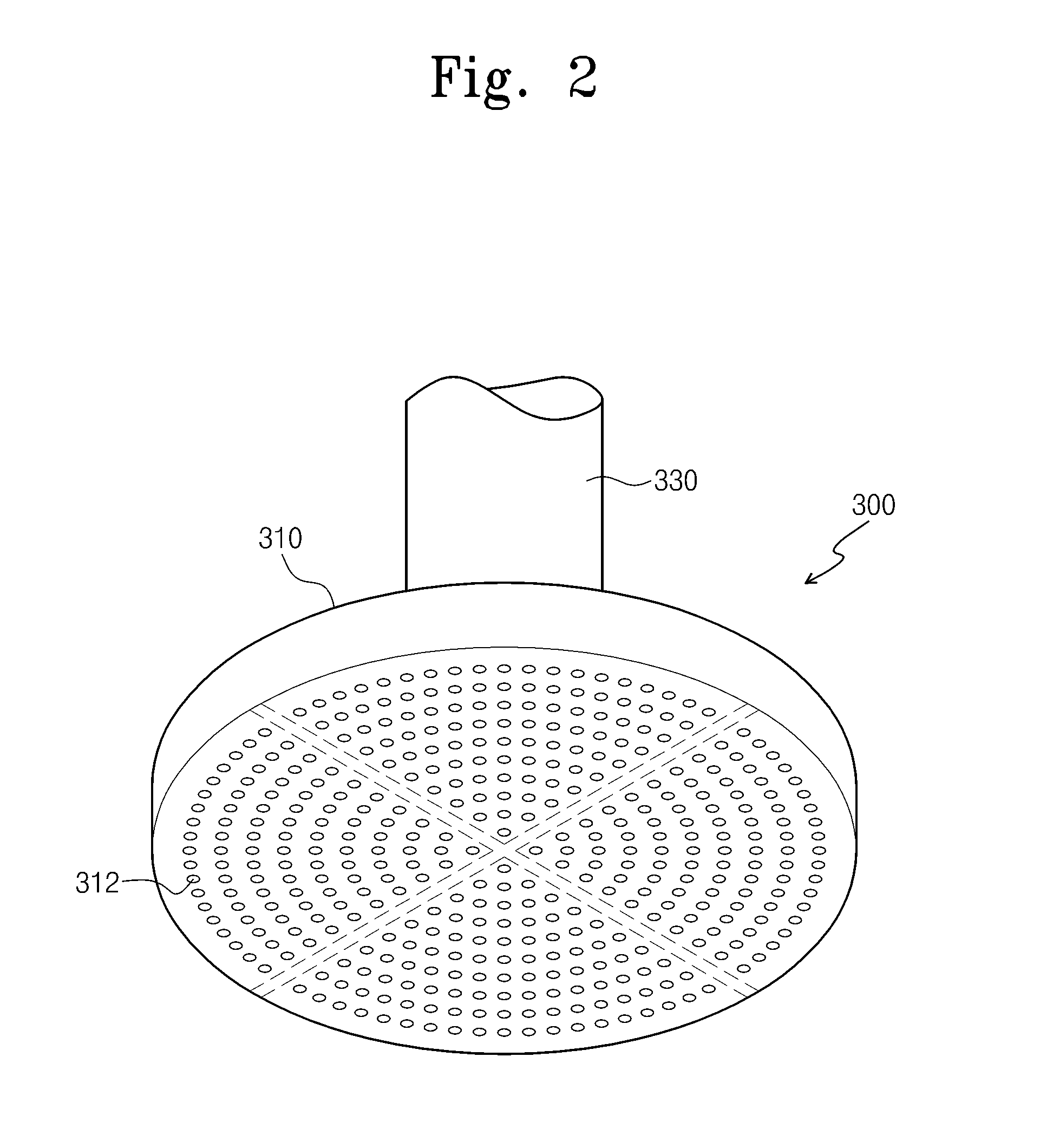
[0030]FIG. 1 is a view of an atomic layer deposition apparatus according to the present invention. FIG. 2 is an exploded perspective view of a spray member of FIG. 1. FIG. 3 is a cross-sectional view of the spray member of FIG. 1. FIG. 4 is a perspective view of a substrate susceptor shown in FIG. 1.

[0031]Referring to FIGS. 1 to 4, an atomic layer deposition apparatus 10 includes a process chamber 100, a substrate susceptor 200 that is a substrate support member, a spray member 300, and a supply member 400.

[0032]The process chamber 100 has an entrance 112 in a side thereof Substrates W may be loaded or unloaded into / from the process chamber 100 through the entrance 112 during the processing. Also, the process chamber 100 includes an exhaust duct 120 and an exhaust tube 114 which exhaust a reaction gas and purge gas, which are supplied therein, and byproducts generated during an atomic layer deposition process at an upper edge thereof The exhaust duct 120 is disposed outside the spra...


PUM

PropertyMeasurementUnit
Angleaaaaaaaaaa
Electrical conductivityaaaaaaaaaa
Areaaaaaaaaaaa

Abstract

The present disclosure relates to a deposition apparatus used to manufacture a semiconductor device including a process chamber; a substrate susceptor installed in the process chamber and including a plurality of concentrically arranged stages on which substrates are positioned; a plurality of members for supplying reaction gas; a member for supplying purge gas; a spray member including a plurality of baffles for independently spraying reaction gas and purge gas, supplied from the plurality of members supplying reaction gas and the member supplying purge gas, on the entirety of the treating surfaces of the substrate, in positions corresponding respectively to the substrates positioned on the stages; and a driving unit for rotating the substrate susceptor or the spray member in order for the baffles of the spray member to sequentially revolve each of the plurality of substrates positioned on the stages.

Description

TECHNICAL FIELD[0001]The present invention disclosed herein relates to an apparatus used to manufacture a semiconductor device, and more particularly, to a susceptor supporting a substrate and an apparatus including the susceptor to perform a deposition process.BACKGROUND ART[0002]In a deposition process of processes for manufacturing a semiconductor device, an atomic layer deposition process is introducing to improve conformability of a deposited layer. The atomic layer deposition process is a process in which a unit reaction cycle for depositing a layer with a thickness similar to that of an atomic layer is repeated to form a deposition layer with a desired thickness. However, according to the atomic layer deposition process, it takes a long time to grow a layer having a desired thickness because a deposition rate is very slow when compared to a chemical vapor deposition process or a sputtering process. Thus, productivity may be decreased.[0003]Furthermore, temperature uniformity ...

Claims


Application Information

Patent Timeline
IPC IPC(8): C23C16/46
CPCC23C16/45551C23C16/45565C23C16/4581H01L21/68771C23C16/46H01L21/67109H01L21/68764C23C16/4584
Inventor PARK, YONG SUNGLEE, SUNG KWANGKIM, DONG YEUL
Owner KOOKJE ELECTRIC KOREA
Features
  • Generate Ideas
  • Intellectual Property
  • Life Sciences
  • Materials
  • Tech Scout
  • Unparalleled Data Quality
  • Higher Quality Content
  • 60% Fewer Hallucinations
Learn More