Thermal Compress Bonding

Active Publication Date: 2013-05-23
TAIWAN SEMICON MFG CO LTD
0 Cites 1 Cited by

AI-Extracted Technical Summary

Problems solved by technology

One of the problems found in the conventional bond structures is that cracking often occurs in solder bumps 104 after the bond...

Abstract

A method includes providing a substrate carrier including work piece holders, and placing a first plurality of work pieces into the work piece holders. A second plurality of work pieces is picked up and placed, with each of the second plurality of work pieces being placed on one of the first plurality of work pieces. Solder bumps between the first and the second plurality of work pieces are then reflowed to simultaneously bond the first and the second plurality of work pieces together.

Application Domain

Semiconductor/solid-state device detailsSolid-state devices +4

Technology Topic

Industrial engineering

Image

  • Thermal Compress Bonding
  • Thermal Compress Bonding
  • Thermal Compress Bonding

Examples

  • Experimental program(1)

Example

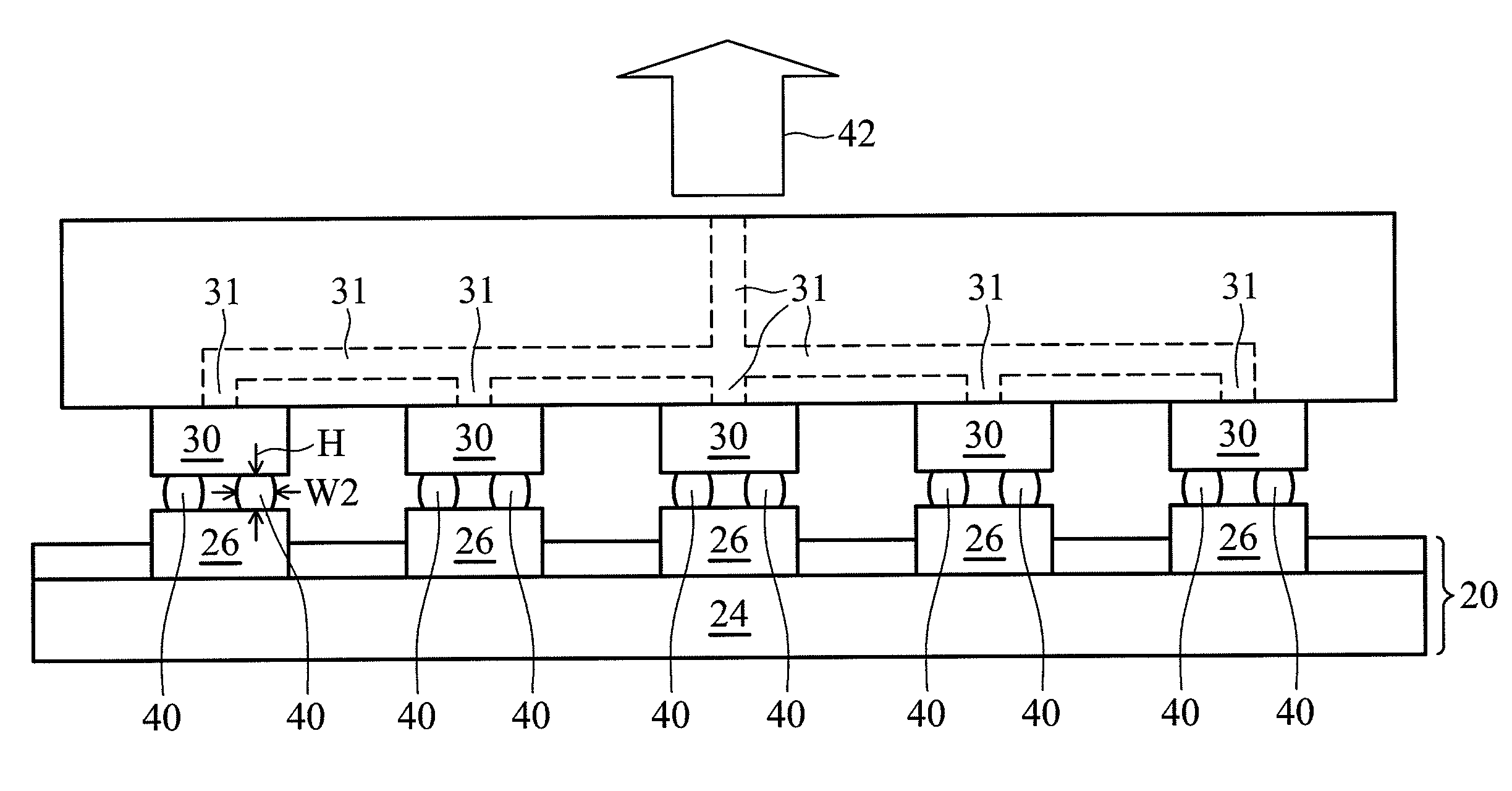
[0012]The making and using of the embodiments of the disclosure are discussed in detail below. It should be appreciated, however, that the embodiments provide many applicable inventive concepts that can be embodied in a wide variety of specific contexts. The specific embodiments discussed are merely illustrative, and do not limit the scope of the disclosure.
[0013]A novel thermal compression bonding (TCB) process is provided. The intermediate stages of manufacturing various embodiments are illustrated. Throughout the various views and illustrative embodiments, like reference numbers are used to designate like elements.
[0014]FIGS. 4A and 4B illustrate a top view and a cross-sectional view, respectively, of substrate carrier 20. Substrate carrier 20 includes a plurality of work piece holders 22, which may be arranged as an array having rows and columns. As shown in FIG. 4B, work piece holders 22 may be holes having the size of work pieces 26 (not shown in FIGS. 4A and 4B, please refer to FIG. 5) that will be placed therein. In an embodiment, heater 24 is placed under, or built in, substrate carrier 20 for heating the work pieces placed in work piece holders 22. In alternative embodiments, substrate carrier 20 includes no heater.
[0015]Referring to FIG. 5, work pieces 26 are placed into work piece holders 22. In an embodiment, work pieces 26 are package substrates or interposers, which do not have active devices such as transistors therein. In alternative embodiments, work pieces 26 are device dies having active devices such as transistors (not shown) therein. Metal bumps 28 are formed on top surfaces of work pieces 26. In an embodiment, all work piece holders 22 are filled with work pieces 26. Alternatively, a part, by not all, of work pieces holders 22 is filled.
[0016]Next, as shown in FIGS. 6A and 6B, work pieces 30 are picked up and placed onto work pieces 26. Metal bumps 32 at bottom surfaces of work pieces 30 are in contact with metal bumps 28. Work pieces 30 may be device dies (chips) comprising active devices (not shown), which may be transistors. Alternatively, work pieces 30 may be interposers, package substrates, or the like. In an embodiment, metal bumps 32 are solder bumps, although they can be other type of bumps such as copper bumps. However, at least one, and may be both, of metal bumps 28 and 32 are solder bumps. In the following illustrated exemplary embodiments, metal bumps 28 and 32 are all solder bumps.
[0017]Heating tool 36 is placed over and contacting work pieces 30, and may apply a downward force (symbolized by arrow 39) on work pieces 30, so that metal bumps 28 and 32 are pressed against each other to prevent work pieces 30 from slipping. In FIG. 6A, heating tool 36 includes a plurality of heating heads 38. When placed over work pieces 30, each of heating heads 38 is aligned to, and contacts, one of work pieces 30. In FIG. 6B, heating tool 36 includes only one heating head that has a size great enough to contact all of work pieces 30.
[0018]Next, as shown in FIG. 7, a bonding is performed. Heating tool 36 heats work pieces 30, and the heat is conducted to, and causing the reflow of, solder bumps 28 and 32. The resulting solder bumps formed of combined solder bumps 28 and 32 are referred to as solder bumps 40. In the embodiment as shown in FIG. 6A, all heating heads 38 are at a same temperature, and hence all of solder bumps 28 and 32 are melted. In the embodiment as shown in FIG. 6B, the surface portions of heating head 38 contacting different work pieces 30 have a substantially uniform temperature, and hence all of solder bumps 28 and 32 are melted substantially simultaneously. During the melting of solder bumps 28 and 32, heating tool 36 (and work pieces 30) may be kept at a fixed level to prevent the melted bumps 28 and 32 from further collapse, which may further cause neighboring bumps 28/32 to short to each other. After the reflow to form solder bumps 40, heating tool 36 applies an upward force, as symbolized by arrow 42, so that heights H of solder bumps 40 are increased, and horizontal sizes W2 of solder bumps 40 are reduced. The application of the upward force may be achieved, for example, by creating a vacuum in heating tool 36 to suck work pieces 30 up, wherein the vacuum may be generated in pipes 31. During the reflow process, heater 24 may have an elevated temperature to heat work pieces 26. Alternatively, heater 24 is not heated. The temperature of heating tool 36 is then lowered until solder bumps 40 solidify. The bonding process is then finished.
[0019]In the embodiments shown in FIGS. 4A through 7, all work pieces on substrate carrier 20 are bonded simultaneously. In alternative embodiments, substrate carrier 20 may be divided into a plurality of zones, with each zone including a plurality of work piece holders 22. The plurality of work pieces in a same zone my be bonded simultaneously using essentially the same methods as shown in FIGS. 4A through 7, while the work pieces in different zones may be bonded in different periods of time.
[0020]By using the embodiments, the throughput of the bonding process is significantly improved. For example, assuming ten chips are to be bonded to ten package substrates, and only one chip is bonded each time. The picking and placing of each chip takes 2 seconds, and the heating and reflowing of each chip takes 30 seconds. The total time required for bonding all 10 chips will be (2+30)×10, which is 320 seconds. As a comparison, by using the embodiments, although the picking and placing of ten chips still take 20 seconds in total, the heating and reflowing of ten chips only take 30 seconds due to the simultaneously reflowing of all chips. The total time is thus only 50 seconds. If more chips are bonded simultaneously, the improvement in the throughput is more significant. Since the cost of the TCB bonding is very high, the reduction in the cost of the bonding process due to the improved throughput is also significant.
[0021]Although the embodiments and their advantages have been described in detail, it should be understood that various changes, substitutions and alterations can be made herein without departing from the spirit and scope of the embodiments as defined by the appended claims. Moreover, the scope of the present application is not intended to be limited to the particular embodiments of the process, machine, manufacture, and composition of matter, means, methods and steps described in the specification. As one of ordinary skill in the art will readily appreciate from the disclosure, processes, machines, manufacture, compositions of matter, means, methods, or steps, presently existing or later to be developed, that perform substantially the same function or achieve substantially the same result as the corresponding embodiments described herein may be utilized according to the disclosure. Accordingly, the appended claims are intended to include within their scope such processes, machines, manufacture, compositions of matter, means, methods, or steps. In addition, each claim constitutes a separate embodiment, and the combination of various claims and embodiments are within the scope of the disclosure.

PUM

PropertyMeasurementUnit
Force
Height

Description & Claims & Application Information

We can also present the details of the Description, Claims and Application information to help users get a comprehensive understanding of the technical details of the patent, such as background art, summary of invention, brief description of drawings, description of embodiments, and other original content. On the other hand, users can also determine the specific scope of protection of the technology through the list of claims; as well as understand the changes in the life cycle of the technology with the presentation of the patent timeline. Login to view more.
Why Eureka
Try Eureka