High-voltage integrated circuit device

a high-voltage integrated circuit and circuit technology, applied in semiconductor devices, process and machine control, instruments, etc., can solve the problems of failure or destruction of hvic b, failure or destruction of chips, etc., to prevent erroneous operation and latchup of logic portions and prevent erroneous operation and destruction of low-side circuit portions

Active Publication Date: 2013-05-23
FUJI ELECTRIC CO LTD
View PDF7 Cites 10 Cited by
  • Summary
  • Abstract
  • Description
  • Claims
  • Application Information

AI Technical Summary

Benefits of technology

[0059]By way of embodiments of the invention, by making a pickup region of the regions fixed at GND potential outside a high-voltage junction terminating region surrounding the high-side circuit portion a universal contact region, the quantity of carriers flowing into the low-side circuit portion can be reduced, and destruction resulting from erroneous operation and latchup of the logic portion of the low-side circuit portion can be prevented.
[0060]Further, by way of embodiments of the invention, by making a pickup region of the regions fixed at the potential of the high-potential side of the power supply of the high-side circuit portion, disposed in the outer peripheral portion of the high-side circuit portion, a universal contact region, the quantity of carriers flowing into the low-side circuit portion can be reduced, and destruction resulting from erroneous operation and latchup of the logic portion of the low-side circuit portion can be prevented.
[0061]By way of embodiments of the invention, there is the advantageous result that erroneous operation and destruction of the low-side circuit portion can be prevented.

Problems solved by technology

When the absolute value of a negative surge voltage VS0 is greatly increased in the negative direction, an overcurrent flows in the HVIC 111 (chip), and as a result erroneous operation of the high-side circuit portion tends to occur, and there is the concern that failure or destruction of the HVIC 111 (chip) may occur.
However, the above-described high-voltage integrated circuit devices of the prior art have the following problems.
Due to this large current, erroneous operation of the HVIC high-side circuit portion and low-side circuit portion may occur, and destruction due to latchup may occur.
Because this resistor is formed in a polysilicon layer, when a large pulse current (several Amperes to several tens of Amperes) due to a negative surge voltage flows transiently in a parasitic diode between the Vs terminal and the ground terminal, there is the concern that the polysilicon layer may be thermally decomposed by the overcurrent, leading to destruction of the HVIC.
However, there is no mention of prevention of erroneous operation of the logic portion of the low-side circuit portion.
Consequently, there is the concern that erroneous operation such as inversion of the output logic of the L-OUT terminal, and destruction resulting from latchup of the low-side circuit portion 91, may occur.

Method used


Image

  • High-voltage integrated circuit device
  • High-voltage integrated circuit device
  • High-voltage integrated circuit device

Examples


embodiment 1

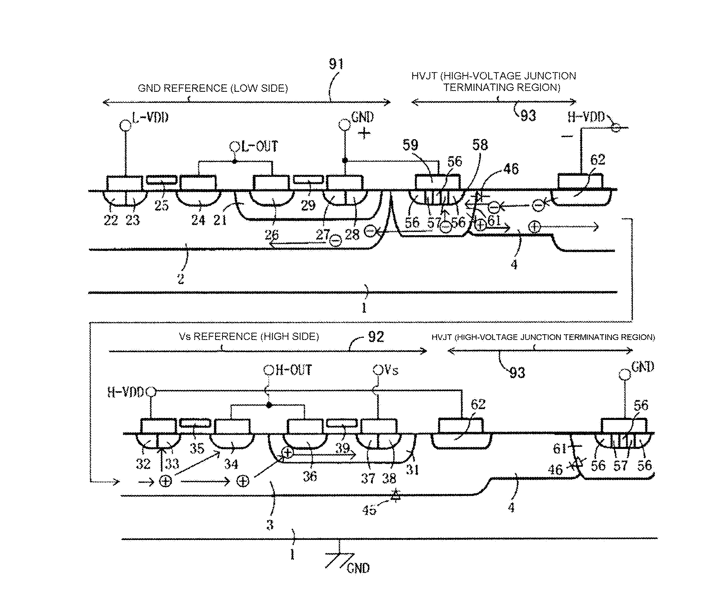
[0079]FIG. 1 is a cross-sectional view showing principal portions of the high-voltage integrated circuit device of Embodiment 1 of the invention. In the high-voltage integrated circuit device 100 shown in FIG. 1, on one of the main faces (hereafter called the surface layer) within a p semiconductor substrate 1 are formed an n region 3 which becomes an n well region, which is a high-side floating potential region; an n− region 4, which becomes a high-voltage junction terminating region 93; and an n− region 2 forming a low-side L-VDD potential region.

[0080]This high-voltage integrated circuit device 100 corresponds to the HVIC 111 which is the driving element shown in FIG. 9, and in particular, corresponds to the low-side circuit portion and high-side circuit portion shown in FIG. 10 controlling the upper-arm IGBT 115 of a half bridge. In FIG. 1, the level-raising circuit is omitted. The level-lowering circuit shown in FIG. 11 can be provided, as necessary, in the high-voltage integra...

embodiment 2

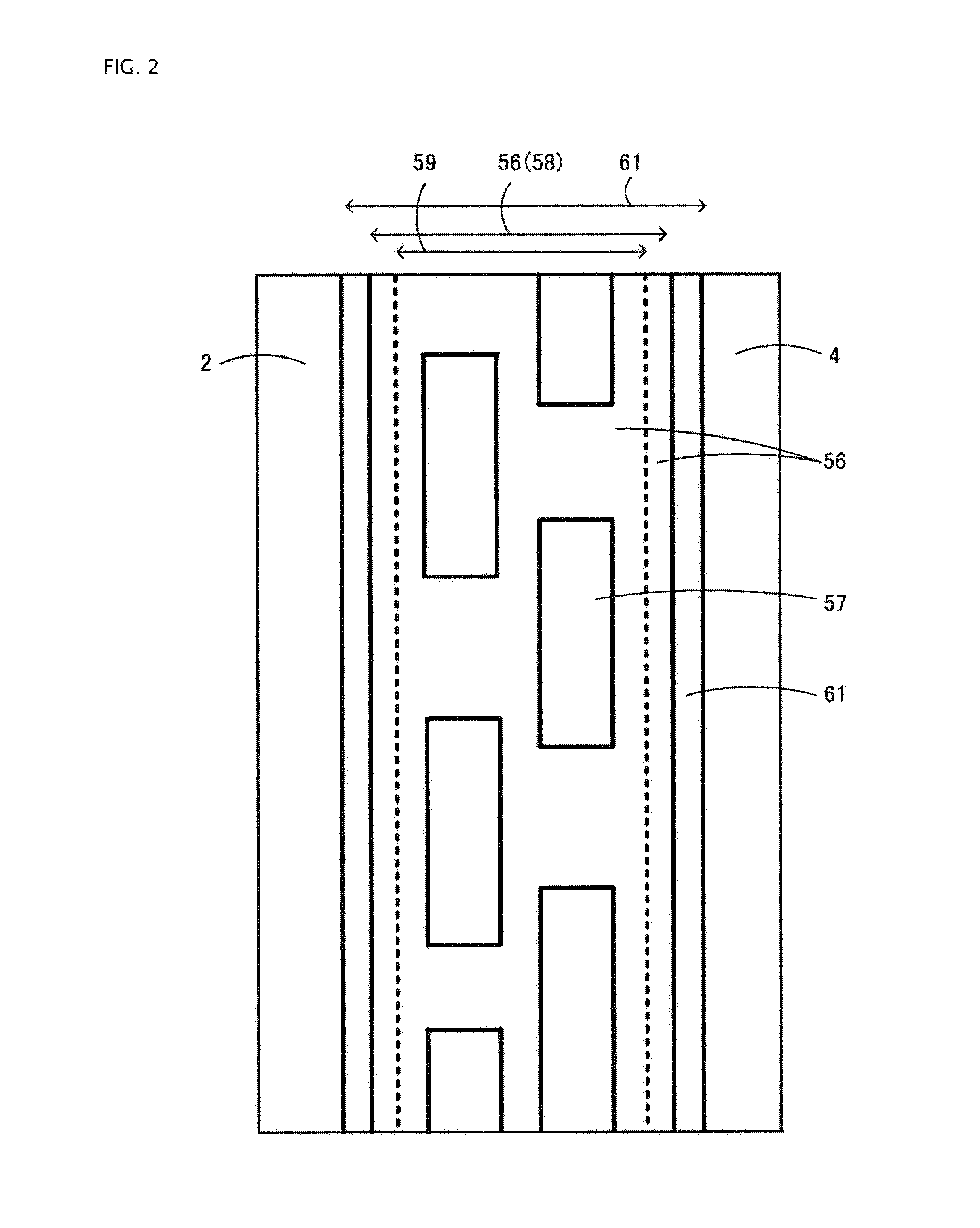
[0108]FIG. 4 is a cross-sectional view showing the principal portions of the high-voltage integrated circuit device of Embodiment 2 of the invention. The high-voltage integrated circuit device 200 of Embodiment 2 differs from the high-voltage integrated circuit device 100 of Embodiment 1 shown in FIG. 1 in that a second universal contact region 68 is also formed under the second pickup electrode 69 connected to the H-VDD terminal. The second universal contact region 68 is formed of n+ regions 62 and p+ regions 63 disposed in mutual alternating contact along the surface of the p semiconductor substrate 1. An explanation is omitted, but the planar pattern of the first universal contact region 58 is the same as the planar pattern (FIG. 2) of the first universal contact region in Embodiment 1.

[0109]FIG. 5 is a plane view showing the planar pattern of the second universal contact region. The second universal contact region 68 has a rectangular planar shape surrounded by the n+ region 62,...

embodiment 3

[0117]FIG. 7 is a cross-sectional view showing the principal portions of the high-voltage integrated circuit device of Embodiment 3 of the invention. A difference between the high-voltage integrated circuit device 300 of Embodiment 3 and the high-voltage integrated circuit device 200 of Embodiment 2 in FIG. 4 is that only the second universal contact region 68 is formed, and a first universal contact region 58 is not formed.

[0118]By forming the second universal contact region 68, when a negative surge voltage is applied to the H-VDD terminal via the Vs terminal, the quantity of electrons injected into the p region 61 is reduced, as explained in Embodiment 2 referring to FIG. 6. As a result, the quantity of electrons flowing into the n− region 2 is reduced, and erroneous operation and destruction due to latchup of the logic portion of the low-side circuit portion 91 can be prevented.

[0119]On the other hand, a portion of the holes injected into the n− region 4 are drawn into the p+ re...


PUM


Abstract

A high-voltage integrated circuit device can include, in a surface layer of a p semiconductor substrate, an n region which is a high-side floating-potential region, an n− region which becomes a high-voltage junction terminating region, and an n− region which is an L-VDD potential region. A low-side circuit portion can be disposed in an n− region. Below a pickup electrode disposed in the high-voltage junction terminating region, a universal contact region in Ohmic contact with the pickup electrode can be disposed. The universal contact region has a p+ region and an n+ region that can be disposed in alternating contact along a surface of the p semiconductor substrate. By disposing the universal contact region in this way, the quantity of carriers flowing into the low-side circuit portion can be reduced when a negative surge voltage is input. Consequently, erroneous operation due to latchup of a logic portion can be minimized.

Description

CROSS-REFERENCE TO RELATED APPLICATIONS[0001]This application is a continuation of International Application No. PCT / JP2012 / 056373, filed on Mar. 13, 2012, which is based on and claims priority to Japanese Patent Application No. JP 2011-056577, filed on Mar. 15, 2011. The disclosure of the Japanese priority application and the PCT application in their entirety, including the drawings, claims, and the specification thereof, are incorporated herein by reference.BACKGROUND[0002]1. Field of the Invention[0003]This invention relates to high-voltage integrated circuit devices.[0004]2. Related Arts[0005]High-voltage integrated circuits (HVICs) are well known as means for on-off driving of switching power devices forming the upper arms of bridge circuits for power inversion (DC-AC conversion) such as PWM inverters. Recently, element separation-type HVICs using high-voltage junctions, not requiring potential insulation by a transformer, photocoupler or similar, have been adopted to enhance f...

Claims


Application Information

Patent Timeline
Patent Type & Authority Applications(United States)
IPC IPC(8): G05F3/02
CPCH01L21/761G05F3/02H01L27/0922H01L27/0921
Inventor YAMAJI, MASAHARU
Owner FUJI ELECTRIC CO LTD
Why Eureka
Try Eureka