Method for producing semiconductor device

Inactive Publication Date: 2013-05-30
NITTO DENKO CORP
View PDF2 Cites 7 Cited by
  • Summary
  • Abstract
  • Description
  • Claims
  • Application Information

AI Technical Summary

Benefits of technology

The patent is about a method for making a semiconductor device that reduces the likelihood of voids during the mounting process, increasing reliability. The method involves using a special connection member and a specific under-fill material that fulfills a certain condition to prevent contamination and ensure good electrical connection between the semiconductor element and the adherend. This condition is satisfied by the relationship between the height of the connection member and the thickness of the under-fill material, which guarantees that the space between the two is filled and prevents excessive protrusion of the under-fill material during the mounting process.

Problems solved by technology

In the above-mentioned process, however, there may arise the following problems.
As a first problem, although it becomes easy to fill a space between an adherend and a semiconductor element, voids (air bubbles) may be generated in a sealing resin during mounting of the semiconductor element at a high temperature, so that protection of the surface of the semiconductor element and connection reliability between the semiconductor element and the adherend become inadequate.
As a result, adjustment of conditions for mounting a semiconductor element becomes severe, and in some cases, joining of a semiconductor element and an adherend is not satisfactorily performed, so that connection reliability between the semiconductor element and the adherend becomes inadequate.

Method used


Image

  • Method for producing semiconductor device
  • Method for producing semiconductor device
  • Method for producing semiconductor device

Examples


first embodiment

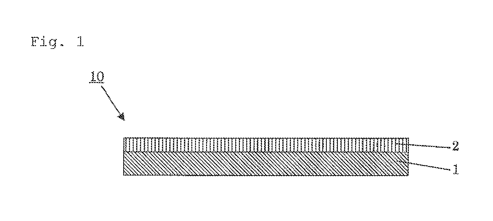
[0040]The present invention is a method for producing a semiconductor device having an adherend, a semiconductor element electrically connected to the adherend, and an under-fill material for filling a space between the adherend and the semiconductor element, in which the method includes the steps of: providing a sealing sheet having a base material and an under-fill material laminated on the base material; bonding the sealing sheet to a surface of a semiconductor wafer on which a connection member is formed; dicing the semiconductor wafer to form a semiconductor element with the under-fill material; retaining the semiconductor element with the under-fill material at 100 to 200° C. for 1 second or more; and electrically connecting the semiconductor element and the adherend through the connection member while filling a space between the adherend and the semiconductor element using the under-fill material. A first embodiment as one embodiment of the present invention will be described...

second embodiment

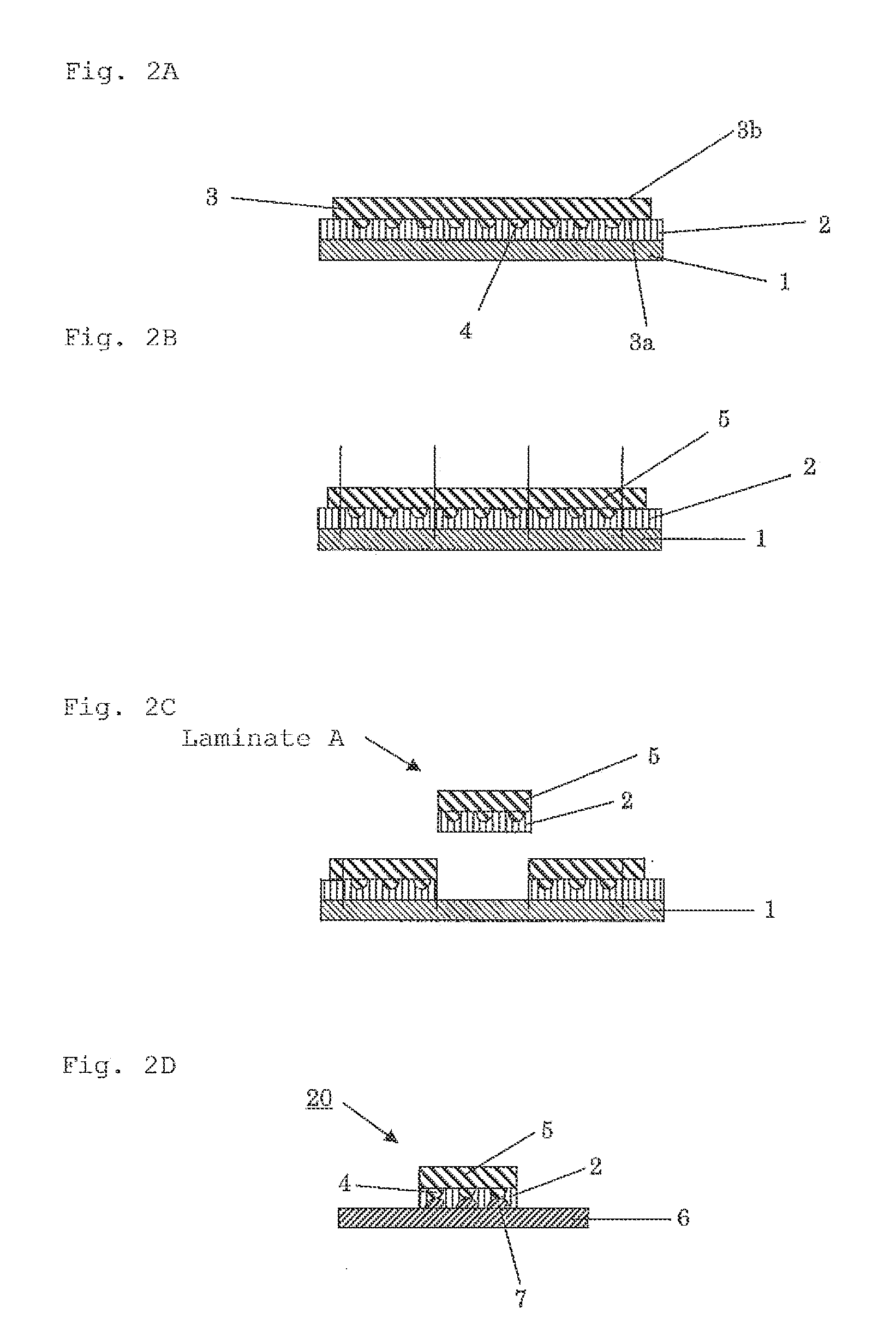
[0105]The present invention is a method for producing a semiconductor device having an adherend, a semiconductor element electrically connected to the adherend, and an under-fill material for filling a space between the adherend and the semiconductor element, in which the method includes: a providing step of providing a sealing sheet having a base material and an under-fill material laminated on the base material; a bonding step of bonding together a surface of a semiconductor wafer, on which a connection member is formed, and the sealing sheet; a dicing step of dicing the semiconductor wafer to form a semiconductor element with the under-fill material; and a connection step of electrically connecting the semiconductor element and the adherend through the connection member while filling a space between the adherend and the semiconductor element using the under-fill material, and the connection step includes the steps of: contacting the connection member and the adherend with each ot...

third embodiment

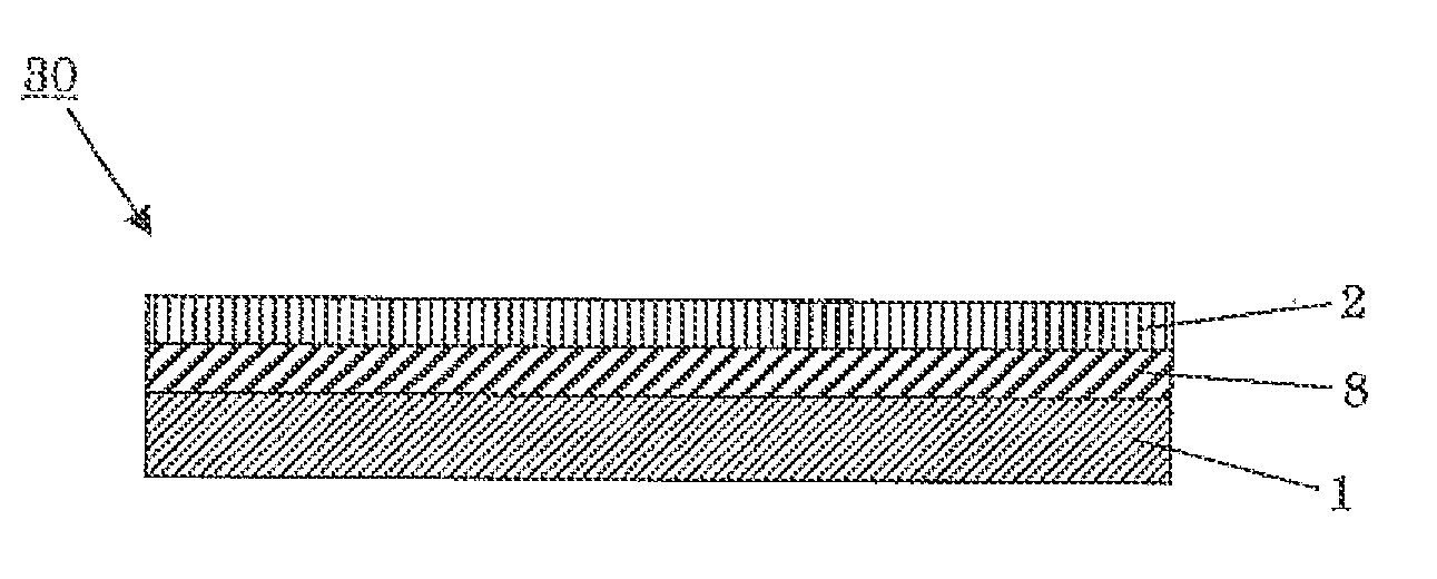
[0118]In the first embodiment, a sealing sheet with an under-fill material laminated directly on a base material is described, but the third embodiment describes a sealing sheet provided with a pressure-sensitive adhesive layer between a base material and an under-fill material. FIG. 3 is a sectional schematic view showing a sealing sheet according to the third embodiment that is another embodiment of the present invention.

[0119]As shown in FIG. 3, the sealing sheet according to the third embodiment includes a base material1, a pressure-sensitive adhesive layer 8 laminated on the base material 1, and an under-fill material 2 laminated on the pressure-sensitive adhesive layer 8. Since the base material 1 and the under-fill material 2 are same as those of the first embodiment, the pressure-sensitive adhesive layer 8 is described here.

(Pressure-Sensitive Adhesive Layer)

[0120]The pressure-sensitive adhesive layer 8 may be formed by a previously known pressure-sensitive adhesive, or may ...


PUM


Abstract

There is provided a method for producing a semiconductor device, which is capable of suppressing voids during mounting of a semiconductor element to produce a semiconductor device with high reliability. A method for producing a semiconductor device of the present invention includes the steps of: providing a sealing sheet having a base material and an under-fill material laminated on the base material; bonding the sealing sheet to a surface of a semiconductor wafer on which a connection member is formed; dicing the semiconductor wafer to form a semiconductor element with the under-fill material; retaining the semiconductor element with the under-fill material at 100 to 200° C. for 1 second or more; and electrically connecting the semiconductor element and the adherend through the connection member while filling a space between the adherend and the semiconductor element with the under-fill material.

Description

BACKGROUND OF THE INVENTION[0001]1. Field of the Invention[0002]The present invention relates to a method for producing a semiconductor device.[0003]2. Description of the Related Art[0004]In recent years, demands for high-density mounting have been increased as electronic instruments have become smaller and thinner. Accordingly, for semiconductor packages, the surface mount type has become mainstream suitable for high-density mounting in place of the conventional pin insertion type. In the surface mount type, a lead is soldered directly to a printed board or the like. For a heating method, the whole of a package is heated by infrared reflow, vapor phase reflow, solder dip or the like to perform mounting.[0005]After surface mounting, a sealing resin is filled in a space between a semiconductor element and a substrate for ensuring protection of the surface of the semiconductor element and connection reliability between the semiconductor element and the substrate. As this sealing resin...

Claims


Application Information

Patent Timeline
IPC IPC(8): H01L21/78
CPCH01L21/78H01L21/563H01L2924/0002H01L2924/00H01L21/50H01L23/28
Inventor SENZAI, HIROYUKITAKAMOTO, NAOHIDEMORITA, KOSUKE
Owner NITTO DENKO CORP
Why Eureka
Try Eureka