
Rotational misalignment measuring device of bonded substrate, rotational misalignment measuring method of bonded substrate, and method of manufacturing bonded substrate

a technology of bonded substrate and measuring device, which is applied in the direction of optical radiation measurement, semiconductor/solid-state device testing/measurement, instruments, etc., can solve the problem of no conventional means to detect such a positional misalignment, and achieve the effect of high accuracy

Active Publication Date: 2013-06-06
KOBE STEEL LTD +1
View PDF4 Cites 38 Cited by
  • Summary
  • Abstract
  • Description
  • Claims
  • Application Information

AI Technical Summary

Benefits of technology

The present invention provides a way to accurately measure the rotation of a bonded substrate, such as a semiconductor wafer, that has been brought together.

Problems solved by technology

In addition, the method described in Japanese Patent Application Laid-open No. 2009-032802 is used for measurement after a bonded wafer has been thinned and cannot be used for measurement at the time of bonding.
However, when a minute positional misalignment occurs during a bonding process, there were no conventional means to detect such a positional misalignment at a micron level.

Method used


Image

  • Rotational misalignment measuring device of bonded substrate, rotational misalignment measuring method of bonded substrate, and method of manufacturing bonded substrate
  • Rotational misalignment measuring device of bonded substrate, rotational misalignment measuring method of bonded substrate, and method of manufacturing bonded substrate
  • Rotational misalignment measuring device of bonded substrate, rotational misalignment measuring method of bonded substrate, and method of manufacturing bonded substrate

Examples


Embodiment Construction

[0030]Hereinafter, an embodiment of the present invention will be described in detail with reference to the drawings. Moreover, in the following embodiment, a substrate according to the present invention will be described as a semiconductor wafer and a bonded substrate according to the present invention will be described as a bonded wafer in which a plurality of semiconductor wafers is bonded to each other. However, it is to be understood that these are merely examples, and since a substrate according to the present invention refers to a disk-like plate constituted by a material such as a semiconductor, glass, and sapphire which is mainly used in an electronic circuit board, a substrate according to the present invention is not limited to a semiconductor wafer.

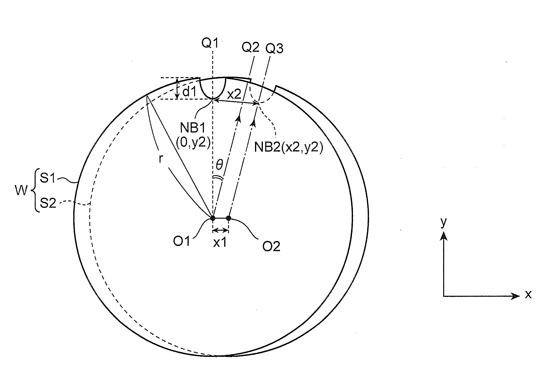
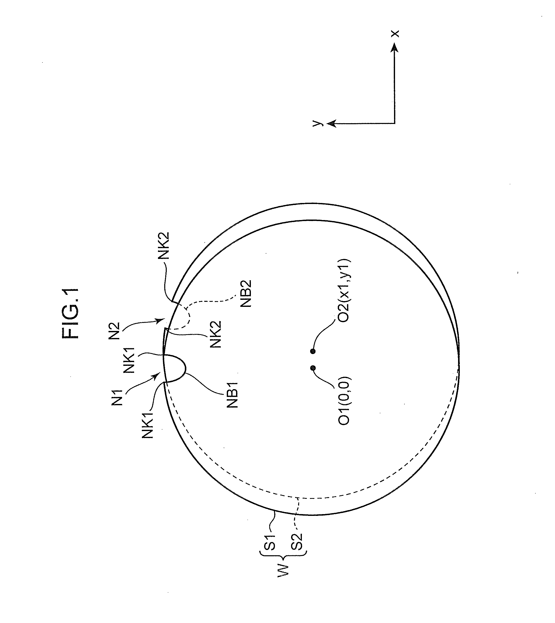
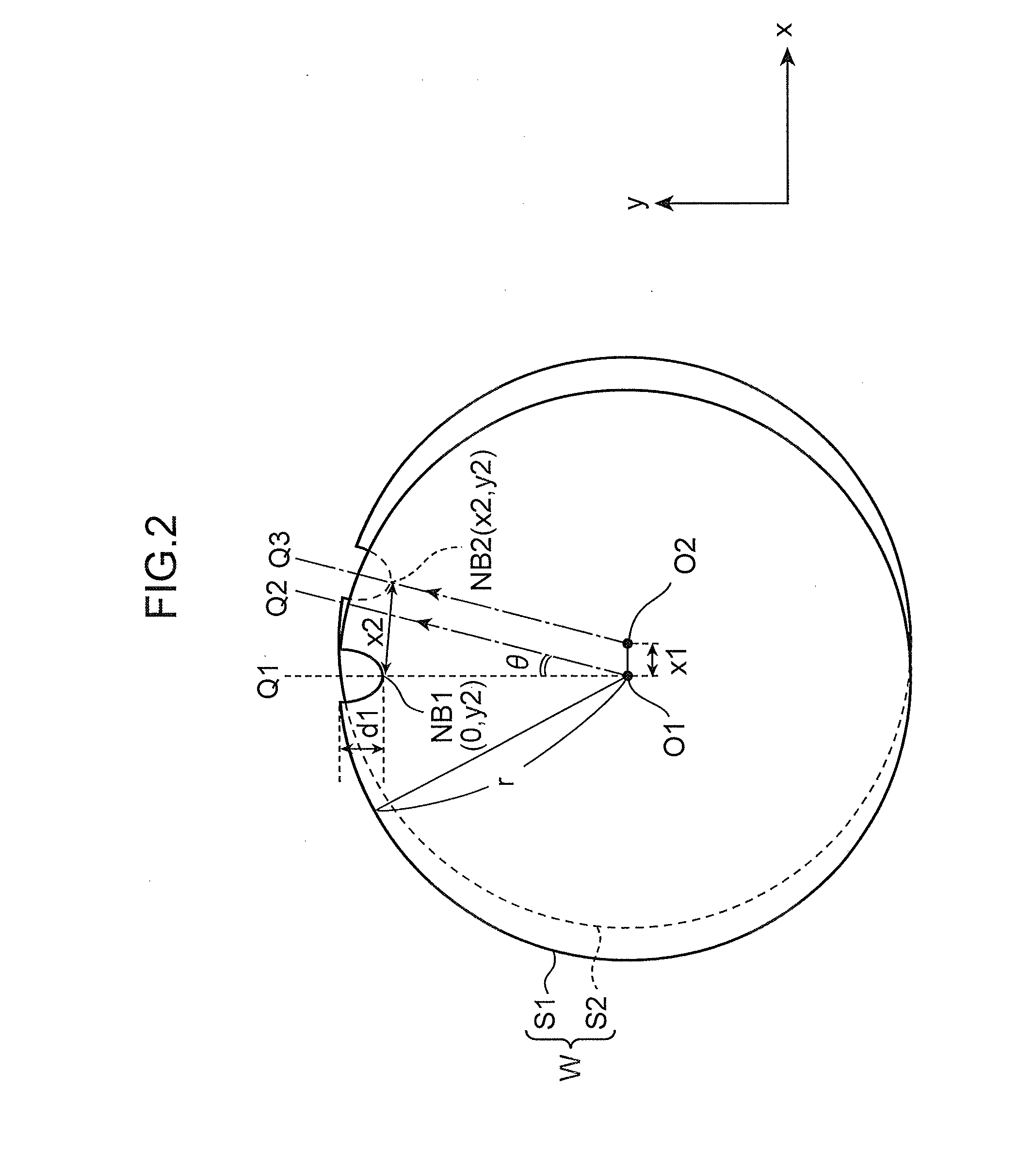
[0031]First, a center position misalignment, a notch position misalignment, and a rotational misalignment between semiconductor wafers constituting a bonded wafer according to the present embodiment will be described. Moreover...


PUM

PropertyMeasurementUnit
thicknessaaaaaaaaaa
angleaaaaaaaaaa
anglesaaaaaaaaaa

Abstract

A rotational misalignment between semiconductor wafers constituting a bonded wafer is calculated. A light source is arranged at a position which is on a front side of an opening of a notch and which is separated from an outer edge portion of a bonded wafer by a predetermined interval, and outputs light to irradiate the outer edge portion of the bonded wafer including the notch. A camera receives and photoelectrically converts reflected light that is specularly-reflected by the outer edge portion of the bonded wafer including the notch among the light outputted by the light source in order to output a brightness distribution of the reflected light as an image. A computer analyzes positions of notches from the image outputted by the camera to obtain a notch position misalignment, and further calculates a rotational misalignment between semiconductor wafers using a center position misalignment between the semiconductor wafers.

Description

BACKGROUND OF THE INVENTION[0001]1. Field of the Invention[0002]The present invention relates to a technique for detecting a rotational misalignment between respective substrates of a bonded substrate in which a plurality of disk-like substrates such as semiconductor wafers each having a notch formed in an outer edge portion thereof is stacked on top of each other and bonded together.[0003]2. Description of the Related Art[0004]With the increases in speed and capacity of semiconductor chips, recently, a technique is known for bonding together a plurality of semiconductor wafers and providing wiring between top and bottom wafers with a through silicon via (TSV). Bonding semiconductor wafers together in this manner requires a technique for accurately bonding the semiconductor wafers to each other in a bonding process. In other words, the semiconductor wafers must be accurately positioned. In order to do so, diameters and center positions of the semiconductor wafers must be accurately ...

Claims


Application Information

Patent Timeline
Patent Type & Authority Applications(United States)
IPC IPC(8): G01B11/27
CPCG01B11/272H01L21/02H01L22/00
Inventor KANNAKA, MASATOKAJITA, MASAKAZUTAKAHASHI, EIJIYAMAMOTO, YUJIAKAMATSU, MASARUIBA, KUNIOIMANISHI, KENJI
Owner KOBE STEEL LTD
Features
  • Generate Ideas
  • Intellectual Property
  • Life Sciences
  • Materials
  • Tech Scout
  • Unparalleled Data Quality
  • Higher Quality Content
  • 60% Fewer Hallucinations
Learn More