
Active matrix organic light-emitting diode display and method for driving the same

a technology of organic light-emitting diodes and active matrix, which is applied in the direction of cathode-ray tube indicators, instruments, electric digital data processing, etc., can solve the problems of circuits that may only be operated at a high power loss, large threshold voltage variations of transistors, and complex and expensive manufacturing processes of active matrix

Inactive Publication Date: 2013-06-06
XU CHIHAO
View PDF6 Cites 31 Cited by
  • Summary
  • Abstract
  • Description
  • Claims
  • Application Information

AI Technical Summary

Benefits of technology

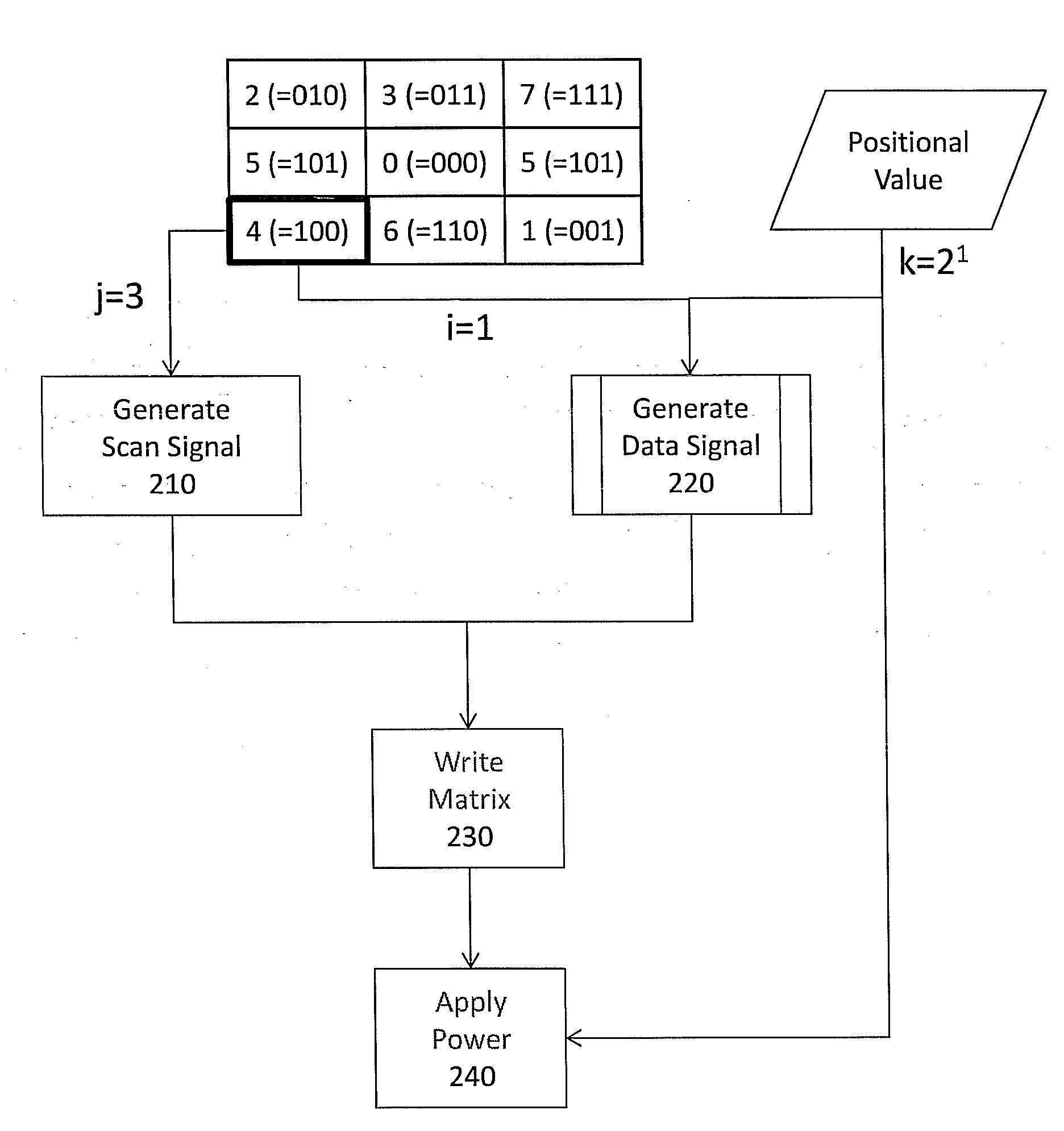
The patent describes methods and devices for driving an active matrix OLED display. The methods involve decomposing image data into subframes based on the physical characteristics of the display, generating binary subframe signals, activating OLED pixels based on a scan signal and a data line signal, and connecting the supply lines to a voltage source for a predetermined duration for each subframe. The devices include a circuit for decomposing image data, a circuit for generating binary subframe signals, a circuit for activating OLED pixels, and a circuit for connecting the supply lines to a voltage source. The methods and devices can improve the display's quality, efficiency, and responsiveness.

Problems solved by technology

But if the active matrix circuit is to be manufactured using a low cost process, transistors may exhibit large variations in their threshold voltage, that may also drift with time.
Moreover, the circuit may only be operated at a high power loss, because a substantial voltage drop at the driving transistor T2 is needed for the current source mode.
This drive scheme, however, is disadvantageous because it is not power efficient and requires a complex and expensive manufacturing process for the active matrix.
A large active-matrix OLED-display is therefore much more expensive than an active-matrix LCD-display.
Consequently, large active-matrix OLED-displays may still not compete with corresponding LCD-displays.

Method used


Image

  • Active matrix organic light-emitting diode display and method for driving the same
  • Active matrix organic light-emitting diode display and method for driving the same
  • Active matrix organic light-emitting diode display and method for driving the same

Examples


Embodiment Construction

[0024]Aspects of the present invention are disclosed in the following description and related figures directed to specific embodiments of the invention. Those skilled in the art will recognize that alternate embodiments may be devised without departing from the spirit or the scope of the claims. Additionally, well-known elements of exemplary embodiments of the invention will not be described in detail or will be omitted so as not to obscure the relevant details of the invention.

[0025]As used herein, the word “exemplary” means “serving as an example, instance or illustration.” The embodiments described herein are not limiting, but rather are exemplary only. It should be understood that the described embodiments are not necessarily to be construed as preferred or advantageous over other embodiments. Moreover, the terms “embodiments of the invention”, “embodiments” or “invention” do not require that all embodiments of the invention include the discussed feature, advantage, or mode of o...


PUM


Abstract

In one exemplary embodiment, a method for driving an AMOLED display having OLED arranged in rows and columns, a pixel circuit for driving an OLED, a scan line for selecting the pixel circuits of each row and a data line for controlling the pixel circuits of each column and supply lines connectable to the anodes and cathodes of the AMOLED pixels may be described. The method may be steps for decomposing image data into a plurality of subframes based on a dependence of physical characteristics of the AMOLED display; generating binary subframe signals according to the decomposed subframes; activating an OLED, based on a scan signal on the scan line and a generated subframe signal applied on the data line, allowing or blocking a current to flow through the organic light emitting diode; and connecting the supply lines to a voltage source for a predetermined duration for each subframe.

Description

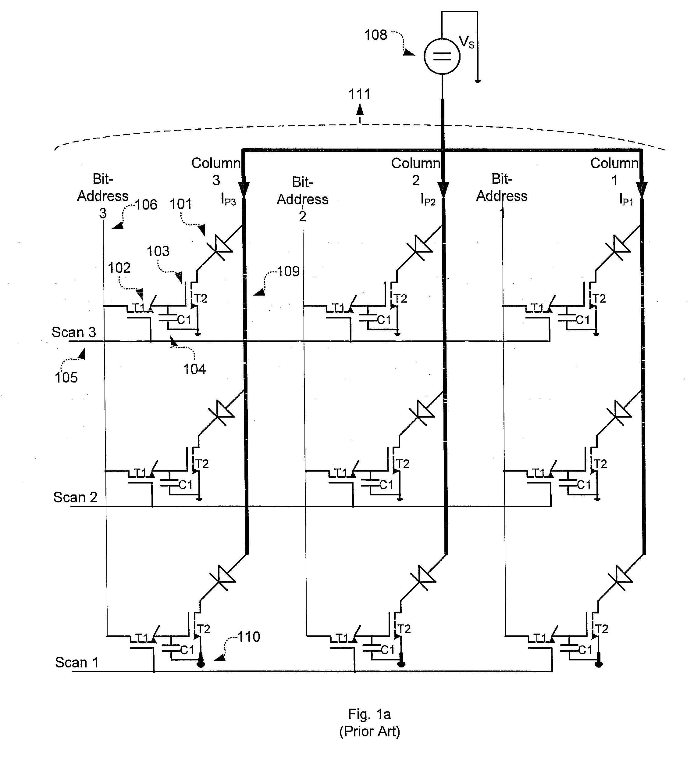
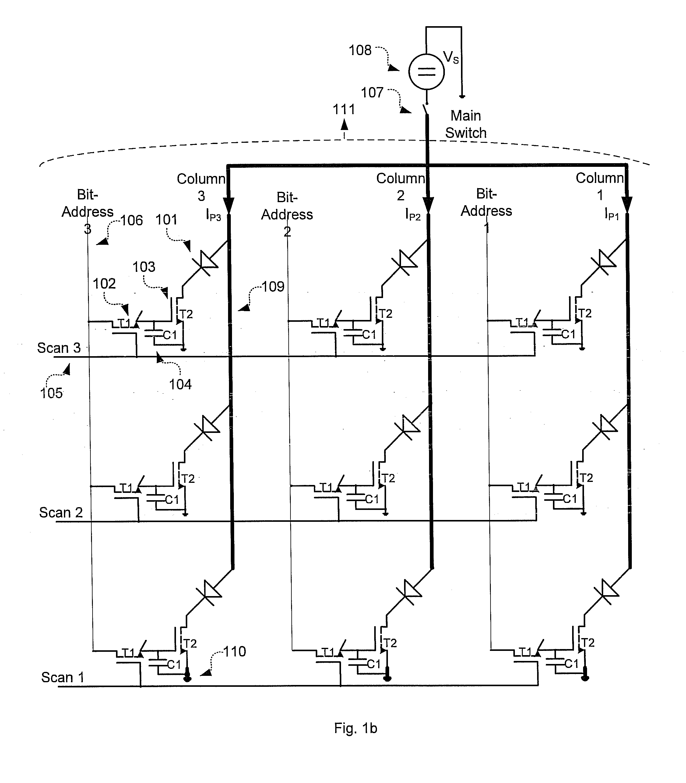
BACKGROUND[0001]In the prior art, there exists a multitude of active matrix circuits for OLED-displays having at least two transistors for each organic light emitting diode, wherein the transistors may be of the same or of a different type (NMOS and PMOS).[0002]Prior art FIG. 1(a) shows a common active matrix circuit for an organic light emitting diode according to the state of the art. Every pixel circuit can have two NMOS transistors T1 (102) and T2 (103), the gate of transistor T1 being connected to the scan-line (105) and the drain of transistor T1 being connected to the data-line (106). The source of T1 is connected to the gate of transistor T2. The capacitor C1 (104) is connected between the gate and the source of T2. Such an active matrix circuit plus the organic light emitting diode (101) is called as AMOLED pixel in this invention. The AMOLED display in FIG. 1(a) (111) can have three rows and three columns and in total of 9 AMOLED pixels.[0003]When the scan-line is activate...

Claims


Application Information

Patent Timeline
Patent Type & Authority Applications(United States)
IPC IPC(8): G09G3/32G09G5/02G09G5/10
CPCG09G3/2022G09G3/2081G09G3/3233G09G2320/045G09G2320/0233G09G2320/0285G09G2320/043G09G2320/0223
Inventor XU, CHIHAO
Owner XU CHIHAO
Learn More