Ultra-small chip package and method for manufacturing the same

a technology of ultra-small chips and chip assemblies, which is applied in the direction of semiconductor devices, semiconductor/solid-state device details, electrical devices, etc., can solve the problems of hampered semiconductor device miniaturization development trend, the volume ratio of the die within the chip package cannot be too high, etc., to reduce the overall volume of the assembly, the effect of substantially the same die size and small volum

Active Publication Date: 2013-06-13
DIODES INC
View PDF1 Cites 4 Cited by
  • Summary
  • Abstract
  • Description
  • Claims
  • Application Information

AI Technical Summary

Benefits of technology

[0016]Note that by attaching both the plate-like back electrode and the plate-like positive electrodes on the surfaces of the die, and directly using the exposed ends of the plate-like electrodes as the lead-out electrodes for the chip assembly, the electrical connections outside of the die only occupy a very small volume. As a result, the proposed technique, while keeping the size of the die substantially the same, can significantly reduce the overall volume of the assembly, thereby enabling the packaging of small or ultra-small chips.

Problems solved by technology

In such designs, the wire-bonding platform and the support platform of the lead-wire frame typically account for a lot of volume within the chip package.
As a result, the volume ratio of the die within the chip package cannot be too high.
These factors have hampered the miniaturization development trend of semiconductor devices.

Method used


Image

  • Ultra-small chip package and method for manufacturing the same
  • Ultra-small chip package and method for manufacturing the same
  • Ultra-small chip package and method for manufacturing the same

Examples


Embodiment Construction

[0028]The following description is presented to enable any person skilled in the art to make and use the embodiments, and is provided in the context of a particular application and its requirements. Various modifications to the disclosed embodiments will be readily apparent to those skilled in the art, and the general principles defined herein may be applied to other embodiments and applications without departing from the spirit and scope of the present disclosure. Thus, the present invention is not limited to the embodiments shown, but is to be accorded the widest scope consistent with the principles and features disclosed herein.

[0029]We now describe detailed embodiments of the design and manufacture of an ultra-small chip assembly in conjunction with the supporting figures.

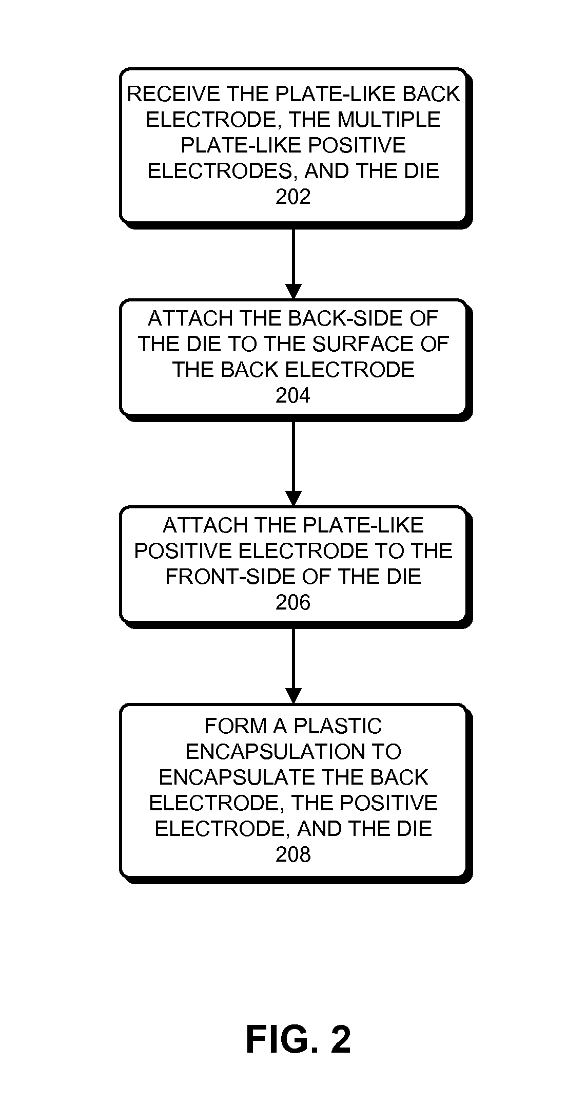
[0030]FIG. 2 presents a flowchart illustrating a process for manufacturing an ultra-small chip assembly in accordance with an embodiment.

[0031]During operation, the process first receives a plate-like back elec...


PUM


Abstract

Some embodiments of the present disclosure provide the design and manufacture of an ultra-small chip assembly. The ultra-small chip assembly comprises a die, a plate-like back electrode disposed on the back-side of the die, and one or more plate-like positive electrodes disposed on the front-side of the die. The ultra-small chip assembly is configured such that one end of the plate-like back electrode extends beyond a first side of the die, and each of the one or more plate-like positive electrodes includes an end which extends beyond a second side of the die. By attaching both the plate-like back electrode and the plate-like positive electrodes on the surfaces of the die, and directly using the exposed ends of the plate-like electrodes as the lead-out electrodes for the chip assembly, the electrical connections outside of the die only occupy a very small volume.

Description

RELATED APPLICATION[0001]This application claims priority under 35 U.S.C. section 119 to Chinese patent application having Application No. 201110401556.8, Publication Serial No. 2011120700615930, entitled “AN ULTRA-SMALL CHIP PACKAGE AND METHOD FOR MANUFACTURING THE SAME,” filed on Dec. 12, 2011, the contents of which are hereby incorporated by reference in their entirety.BACKGROUND[0002]1. Field[0003]This disclosure generally relates to the field of semiconductor device packaging. More specifically, this disclosure relates to an ultra-small chip assembly and method for manufacturing an ultra-small chip assembly.[0004]2. Related Art[0005]As semiconductor devices continue to shrink in size, in order to reduce the overall device size after packaging, it is necessary to increase the volume ratio that is shared by chips in the package.[0006]In traditional semiconductor devices, the chip or die is first affixed onto a support platform of the lead-wire frame of the chip package, and a set...

Claims


Application Information

Patent Timeline
Patent Type & Authority Applications(United States)
IPC IPC(8): H01L23/498
CPCH01L2224/48247H01L24/29H01L23/492H01L23/49562H01L2224/2929H01L2224/33181H01L23/3107H01L2224/48091H01L24/33H01L2224/291H01L2924/1815H01L2924/00015H01L2924/014H01L2924/00014H01L2924/07802
Inventor GAO, HONGTAOZHANG, JIANG YUAN
Owner DIODES INC
Why Eureka
Try Eureka