Semiconductor device and display device including the same

Active Publication Date: 2013-06-20
SEMICON ENERGY LAB CO LTD
View PDF8 Cites 33 Cited by
  • Summary
  • Abstract
  • Description
  • Claims
  • Application Information

AI Technical Summary

Benefits of technology

[0027]In particular, by using a semiconductor device having the above structure as pixel switching elements in a pixel portion, the aperture ratio can be improved and thus higher resolution can be achieved.
[0028]A semiconductor device in which the area of a region where transistors are disposed is reduced can be provided

Problems solved by technology

When the number of the transistors is increased, the area of a region where the transistors are disposed is increased a

Method used


Image

  • Semiconductor device and display device including the same
  • Semiconductor device and display device including the same
  • Semiconductor device and display device including the same

Examples


Example

Embodiment 1

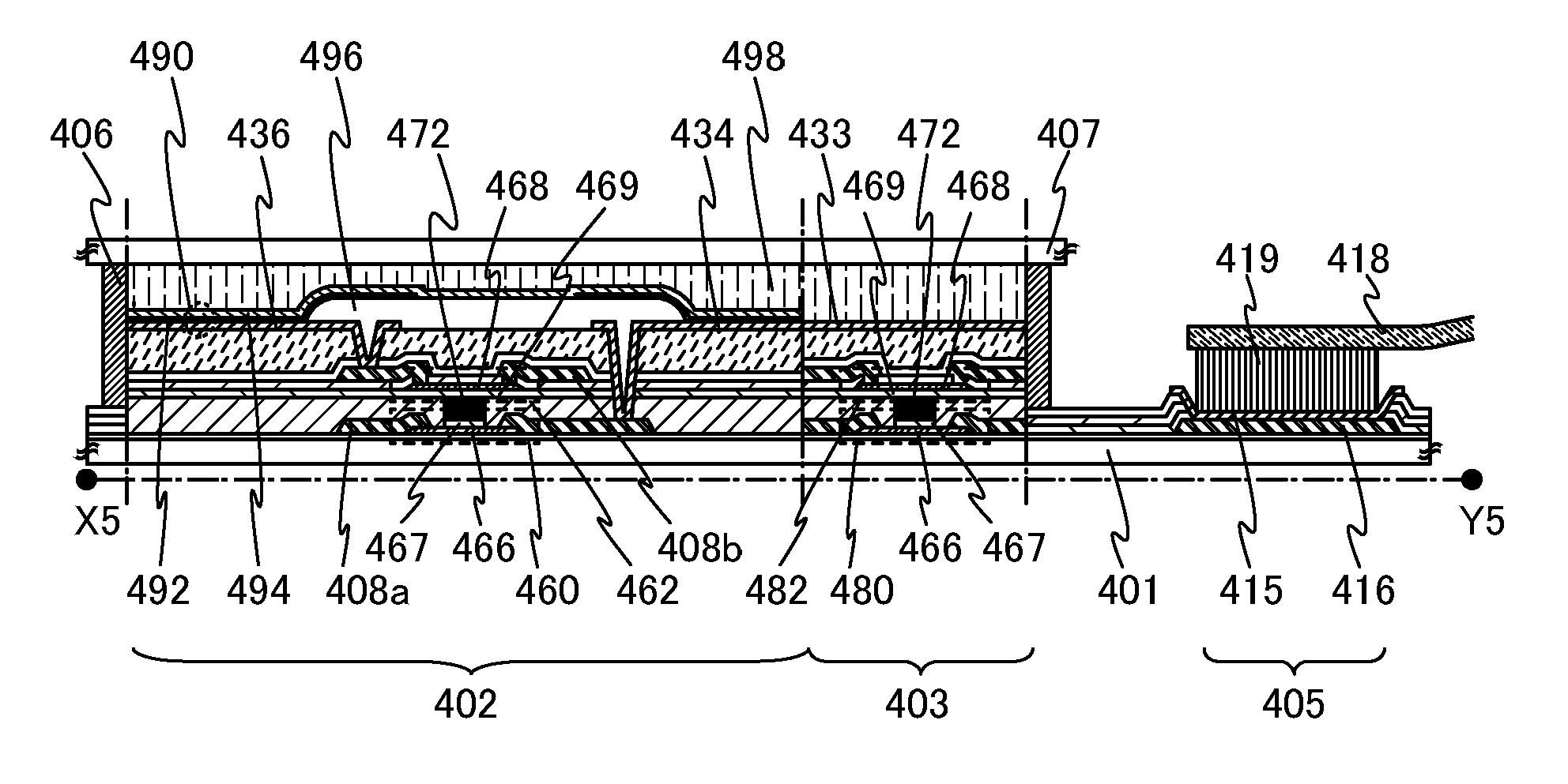
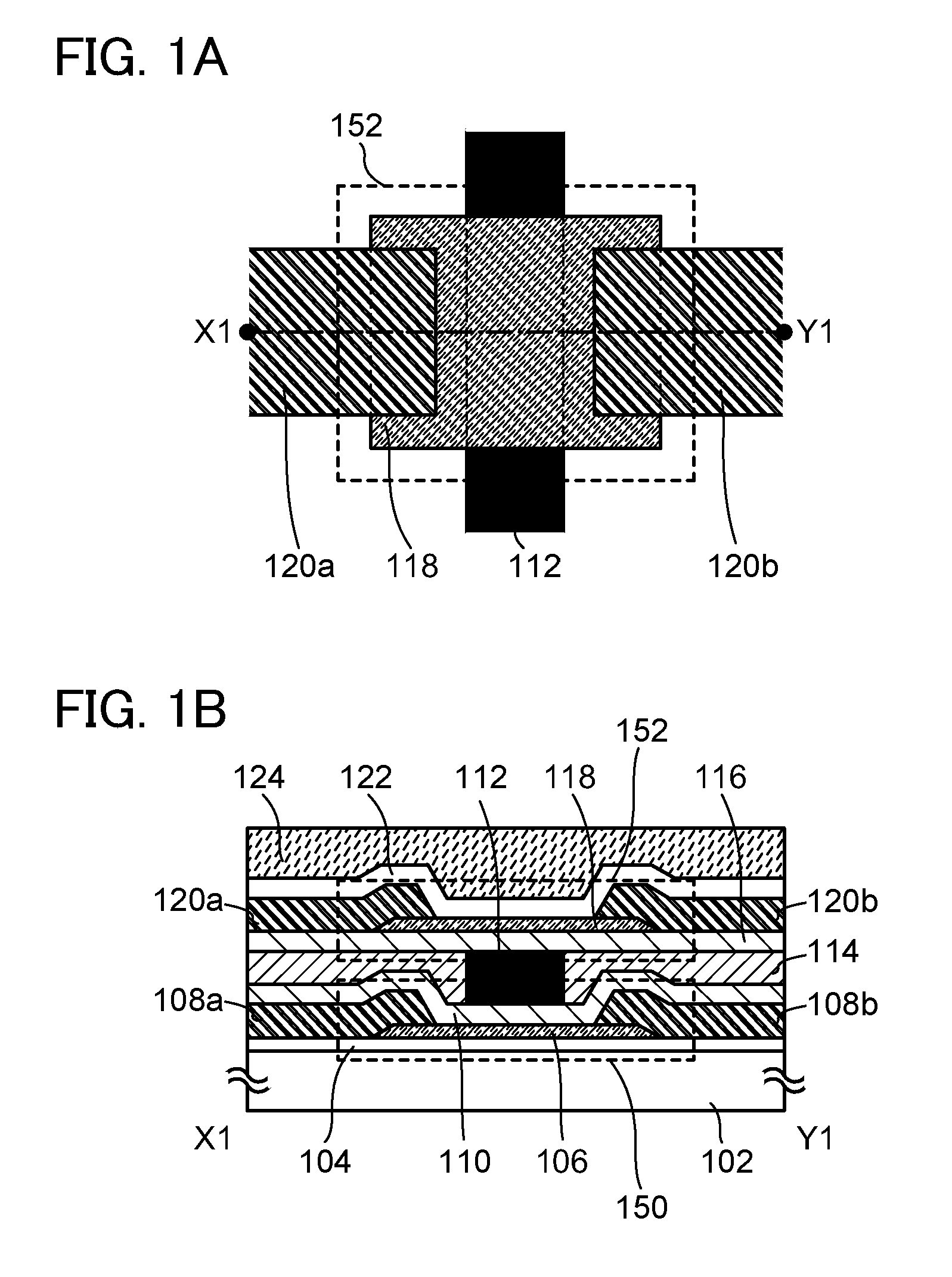
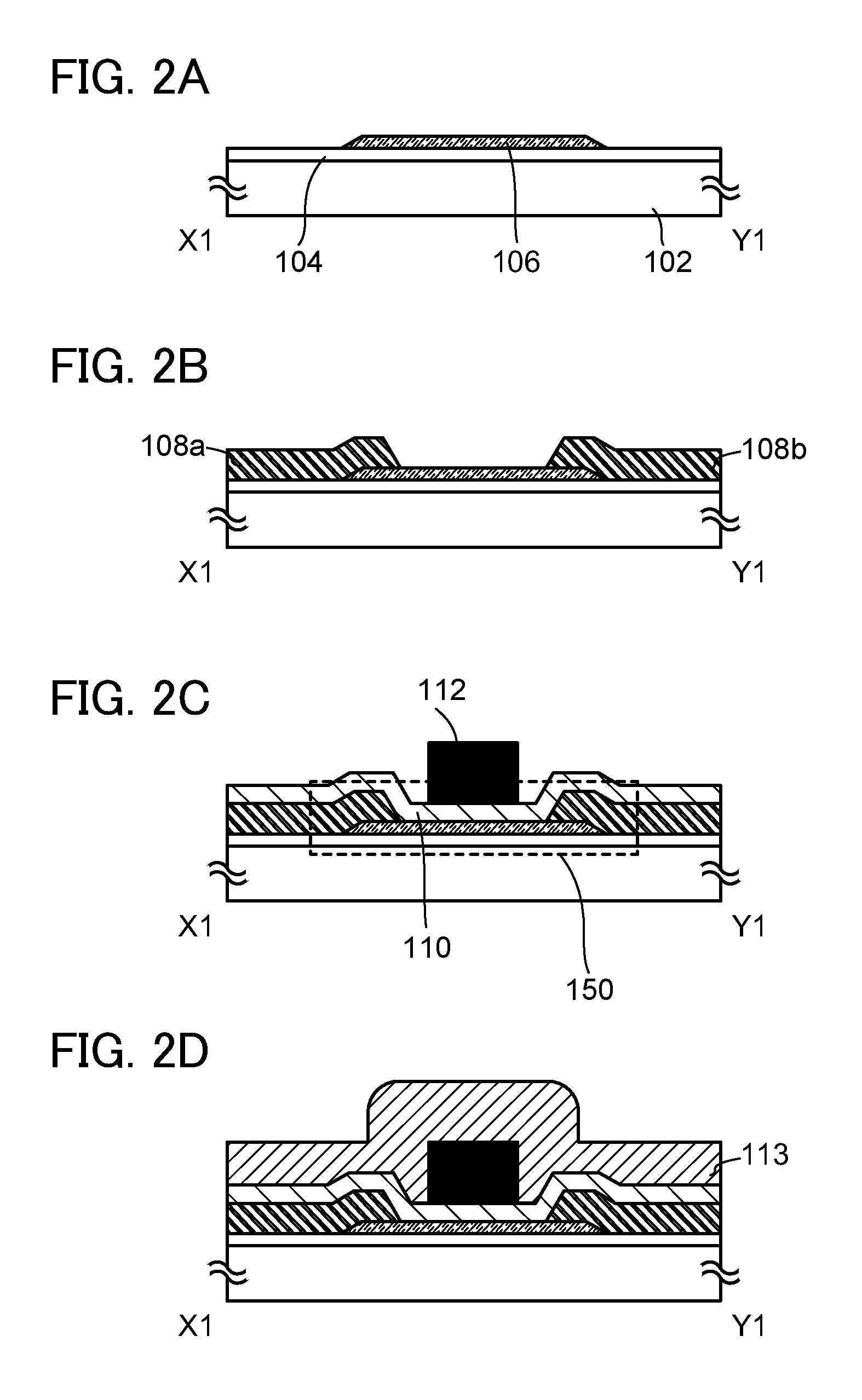
[0048]In this embodiment, one embodiment of a semiconductor device and a method of manufacturing the semiconductor device will be described with reference to FIGS. 1A and 1B, FIGS. 2A to 2D, and FIGS. 3A to 3D.

[0049]FIGS. 1A and 1B are a top view and a cross-sectional view, respectively, of a transistor as one embodiment of a semiconductor device. Note that FIG. 1A is a top view, and FIG. 1B is a cross-sectional view taken along line X1-Y1 in FIG. 1A. Note that in FIG. 1A, some components of the transistor (e.g., a first gate insulating film 110) are not illustrated for simplicity.

[0050]The semiconductor device illustrated in FIGS. 1A and 1B includes a first transistor 150 and a second transistor 152. The first transistor 150 includes a base insulating film 104 formed over a substrate 102; a first semiconductor film 106 formed over the base insulating film 104; a first source electrode 108a and a first drain electrode 108b formed over the first semiconductor film 106; th...

Example

Embodiment 2

[0143]In this embodiment, a modification example of the semiconductor device illustrated in FIGS. 1A and 1B of Embodiment 1 and a manufacturing method which is different from the manufacturing method of the semiconductor device illustrated in FIGS. 2A to 2D and FIGS. 3A to 3D of Embodiment 1 will be described with reference to FIGS. 4A and 4B, FIGS. 5A to 5D, and FIGS. 6A to 6D. Note that portions similar to those in FIGS. 1A and 1B, FIGS. 2A to 2D, and FIGS. 3A to 3D are denoted by the same reference numerals, and description thereof is skipped.

[0144]FIGS. 4A and 4B are a top view and a cross-sectional view, respectively, of a transistor as one embodiment of a semiconductor device. Note that FIG. 4A is a top view, and FIG. 4B is a cross-sectional view taken along line X2-Y2 in FIG. 4A. Note that in FIG. 4A, some components of the transistor (e.g., the first gate insulating film 110) are not illustrated for simplicity.

[0145]The semiconductor device illustrated in FIGS. 4...

Example

Embodiment 3

[0175]In this embodiment, a modification example of the semiconductor device illustrated in FIGS. 1A and 1B of Embodiment 1, or a modification example of the semiconductor device illustrated in FIGS. 4A and 4B of Embodiment 2 will be described with reference to FIGS. 7A and 7B. Note that portions similar to those in FIGS. 1A and 1B and FIGS. 4A and 4B are denoted by the same reference numerals, and description thereof is skipped.

[0176]FIGS. 7A and 7B are a top view and a cross-sectional view, respectively, of a transistor as one embodiment of a semiconductor device. Note that FIG. 7A is a top view, and FIG. 7B is a cross-sectional view taken along line X3-Y3 in FIG. 7A. Note that in FIG. 7A, some components of the transistor (e.g., the first gate insulating film 110) are not illustrated for simplicity.

[0177]The semiconductor device illustrated in FIGS. 7A and 7B includes a first transistor 170 and a second transistor 172. The first transistor 170 includes the base insula...


PUM


Abstract

A first transistor and a second transistor are stacked. The first transistor and the second transistor have a gate electrode in common. At least one of semiconductor films used in the first transistor and the second transistor is an oxide semiconductor film. With the use of the oxide semiconductor film as the semiconductor film in the transistor, high field-effect mobility and high-speed operation can be achieved. Since the first transistor and the second transistor are stacked and have the gate electrode in common, the area of a region where the transistors are disposed can be reduced.

Description

BACKGROUND OF THE INVENTION[0001]1. Field of the Invention[0002]One embodiment of the disclosed invention relates to a semiconductor device and a display device including the semiconductor device.[0003]2. Description of the Related Art[0004]Attention has been focused on a technique for forming a transistor (also referred to as thin film transistor (TFT)) using a semiconductor thin film formed over a substrate having an insulating surface. The transistor is applied to a wide range of electronic devices such as an integrated circuit (IC) and an image display device (display device).[0005]A technique for forming a pixel portion and a driver circuit portion using transistors over the same substrate in a display device has been actively developed.[0006]A silicon-based semiconductor material is widely known as a material for a semiconductor thin film applicable to a transistor. As another material for a semiconductor thin film, an oxide semiconductor material has been attracting attention...

Claims


Application Information

Patent Timeline
IPC IPC(8): H01L29/786
CPCH01L27/1225H01L29/786
Inventor YONEDA, SEIICHI
Owner SEMICON ENERGY LAB CO LTD
Why Eureka
Try Eureka