Carrier, semiconductor package and fabrication method thereof

Active Publication Date: 2013-07-25
SILICONWARE PRECISION IND CO LTD
View PDF9 Cites 5 Cited by
  • Summary
  • Abstract
  • Description
  • Claims
  • Application Information

AI Technical Summary

Benefits of technology

[0021]Therefore, through the design of the concave portion on the carrier, the present invention facilitates alignment of the chip so as to prevent it from displacement that may otherwise impose difficulty in subsequent fabrication processes such as a circuit built-up process and reduce the prod

Problems solved by technology

However, when the chips 12 are disposed on the plate-shaped carrier 10 having the thermal adhesive layer 11, it is difficult to align the chips 12 on the carrier, thus easily causing displacement of the chips 12 and reducing t

Method used


Image

  • Carrier, semiconductor package and fabrication method thereof
  • Carrier, semiconductor package and fabrication method thereof
  • Carrier, semiconductor package and fabrication method thereof

Examples


Example

[0025]The following illustrative embodiments are provided to illustrate the disclosure of the present invention, these and other advantages and effects can be apparent to those in the art after reading this specification.

[0026]It should be noted that the drawings are only for illustrative purposes and not intended to limit the present invention. Meanwhile, terms such as ‘on’, ‘a’ etc. are only used as a matter of descriptive convenience and not intended to have any other significance or provide limitations for the present invention.

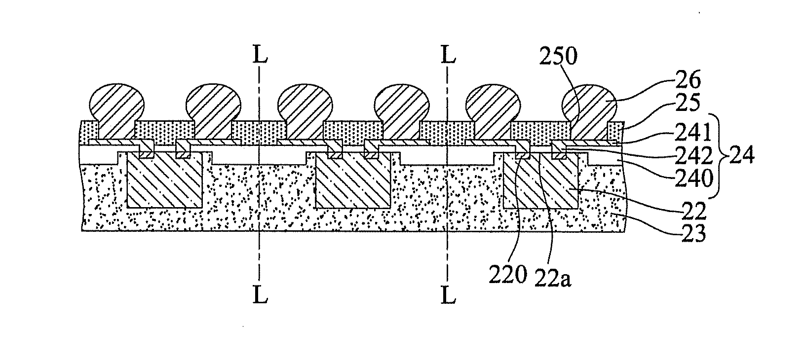
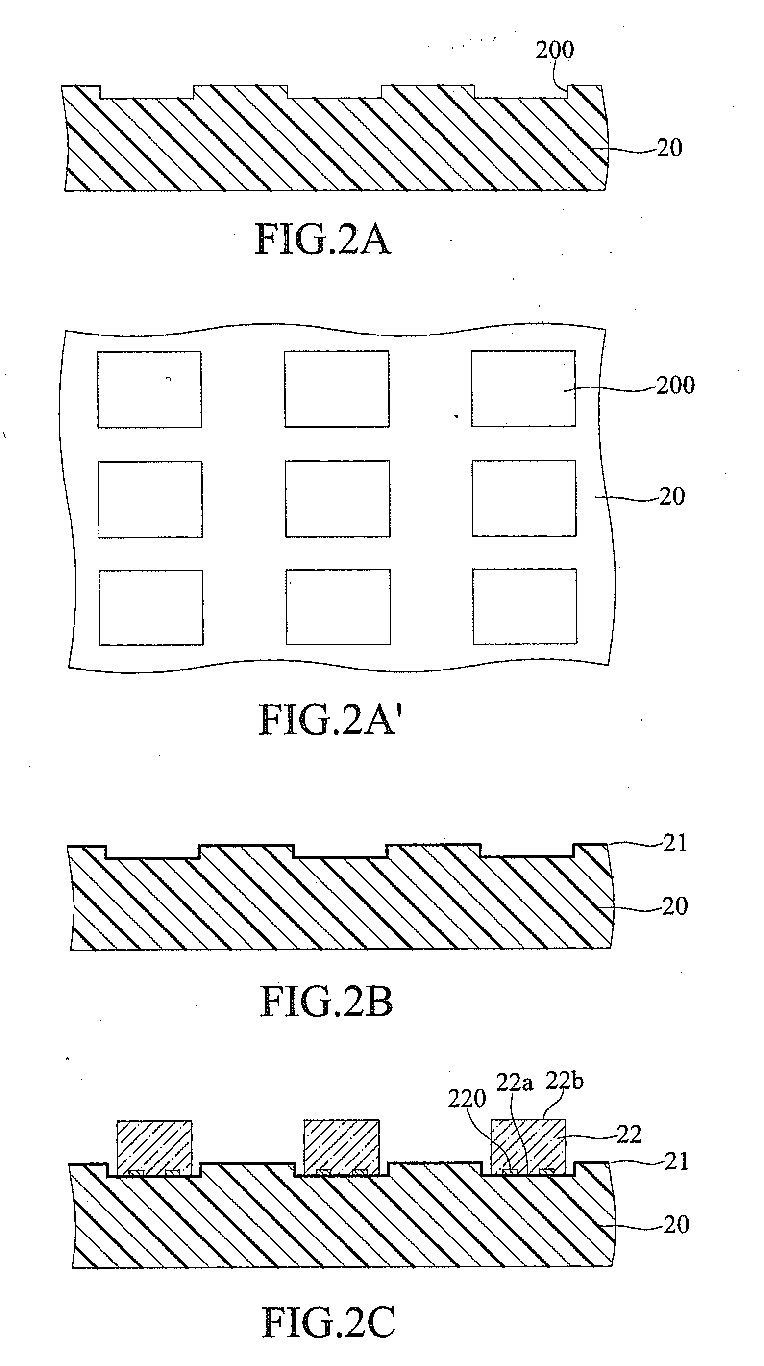
[0027]FIGS. 2A to 2G are schematic cross-sectional views showing a fabrication method of a semiconductor package 2 according to the present invention.

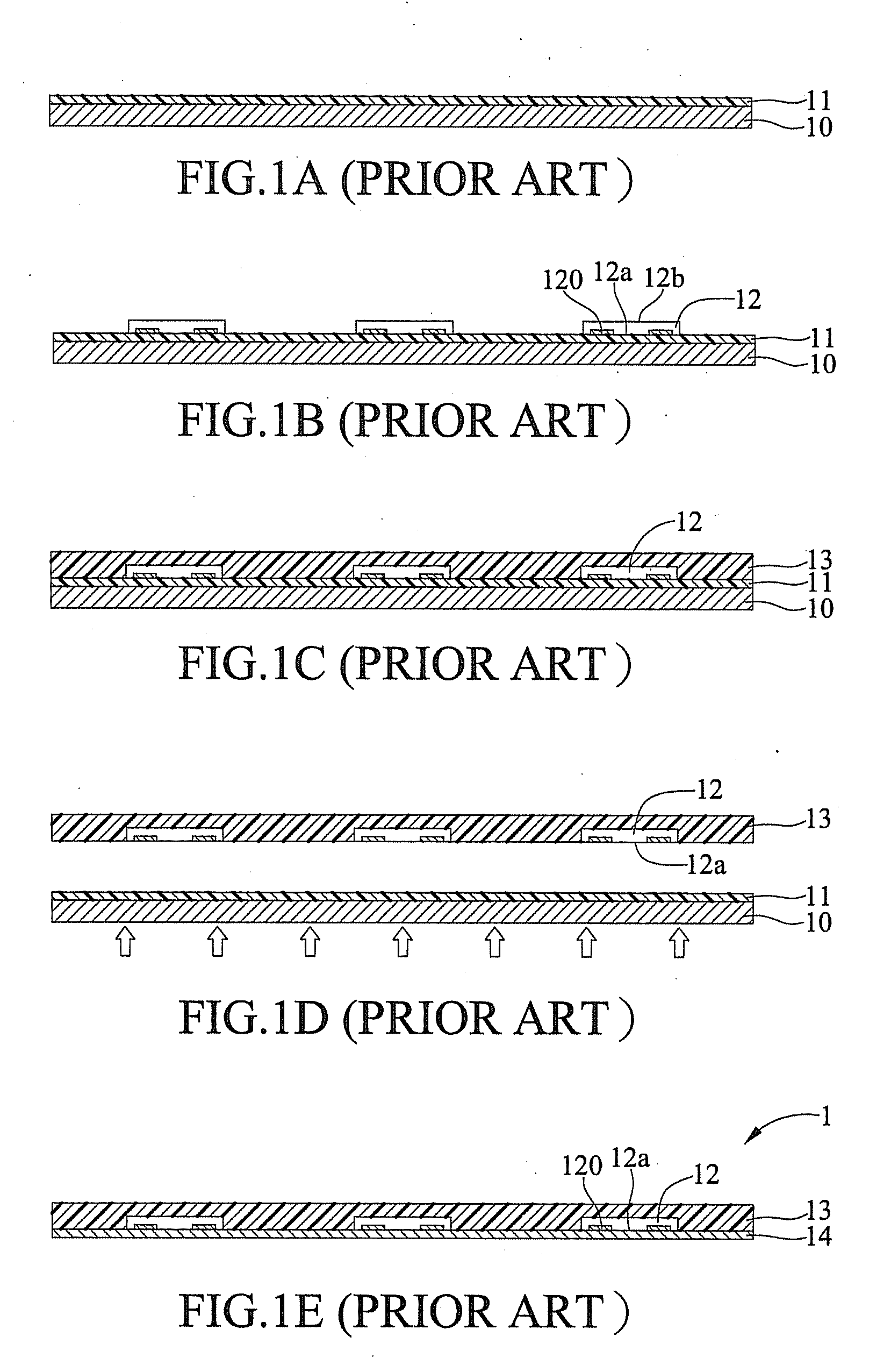
[0028]Referring to FIGS. 2A and 2A′, a carrier 20 having a plurality of concave portions 200 is provided. In the present embodiment, the carrier 20 is made of glass or metal, and the concave portions 200 are array arranged on the carrier 20.

[0029]Referring to FIG. 2B, a releasing layer 21 is formed on the ca...


PUM


Abstract

A fabrication method of a semiconductor package includes the steps of: providing a carrier having a concave portion and a releasing layer formed on a surface thereof; disposing a chip on the releasing layer in the concave portion; forming an encapsulant on the chip and the releasing layer; removing the releasing layer and the carrier; and forming a circuit structure on the encapsulant and the chip. The design of the concave portion facilitates alignment of the chip to prevent it from displacement, thereby improving the product reliability. A semiconductor package fabricated by the fabrication method is also provided.

Description

BACKGROUND OF THE INVENTION[0001]1. Field of the Invention[0002]The present invention relates to semiconductor packages and fabrication methods thereof, and more particularly, to a semiconductor package having an embedded chip and a fabrication method thereof.[0003]2. Description of Related Art[0004]Along with the rapid development of electronic industries, electronic products are developed towards multi-function and high performance. To meet the miniaturization requirement of semiconductor packages, wafer level packaging (WLP) technologies have been developed.[0005]U.S. Pat. No. 6,452,265 and No. 7,202,107 provide fabrication methods of wafer-level packages. FIGS. 1A to 1E are cross-sectional views showing a fabrication method of a semiconductor package 1 according to the prior art.[0006]Referring to FIG. 1A, a thermal adhesive layer 11 is formed on a carrier 10.[0007]Referring to FIG. 1B, a plurality of chips 12 are disposed on the thermal adhesive layer 11. Each of the chips 12 h...

Claims


Application Information

Patent Timeline
IPC IPC(8): H01L23/48H01L21/50H01L21/56
CPCH01L2224/02379H01L24/96H01L21/561H01L24/05H01L24/13H01L2224/05548H01L2224/13022H01L2224/13024H01L2224/131H01L2224/96H01L23/3114H01L24/19H01L2224/0401H01L2924/1815H01L2224/12105H01L2224/04105H01L21/56H01L21/673H01L21/76877H01L21/78H01L21/568H01L2224/11H01L2224/03H01L2924/014H01L21/68H01L21/566H01L21/67333H01L21/4832H01L21/683H01L21/67763H01L2224/97H01L23/31H01L23/3121H01L23/3107
Inventor CHANG, CHIANG-CHENGLEE, MENG-TSUNGHUANG, JUNG-PANGCHIU, SHIH-KUANG
Owner SILICONWARE PRECISION IND CO LTD
Why Eureka
Try Eureka