Semiconductor light emitting apparatus, image displaying apparatus, mobile terminal, head-up display apparatus, image projector, head-mounted display apparatus, and image forming apparatus

a technology of semiconductors and light emitting devices, applied in the direction of static indicating devices, instruments, solid-state devices, etc., can solve the problems of reducing the efficiency of light extraction, reducing the internal quantum efficiency of led chips, and increasing heat generation. , to achieve the effect of minimizing heat generation

Active Publication Date: 2013-08-15
OKI ELECTRIC IND CO LTD
View PDF5 Cites 51 Cited by
  • Summary
  • Abstract
  • Description
  • Claims
  • Application Information

AI Technical Summary

Benefits of technology

[0007]An object of the invention is to minimizing heat generation from the light emitt

Problems solved by technology

However, larger currents flowing through the LEDs and the first and second wirings will seriously increase heat generated due to electrical resistances thereof.
An increased amount of heat causes a decreased internal quantum efficiency of LED chips.
However, the method disclosed in Japanese Patent Publication No. 2002-278481 suffers from the following drawbacks.
If the light emitting chips have not

Method used


Image

  • Semiconductor light emitting apparatus, image displaying apparatus, mobile terminal, head-up display apparatus, image projector, head-mounted display apparatus, and image forming apparatus
  • Semiconductor light emitting apparatus, image displaying apparatus, mobile terminal, head-up display apparatus, image projector, head-mounted display apparatus, and image forming apparatus
  • Semiconductor light emitting apparatus, image displaying apparatus, mobile terminal, head-up display apparatus, image projector, head-mounted display apparatus, and image forming apparatus

Examples


first embodiment

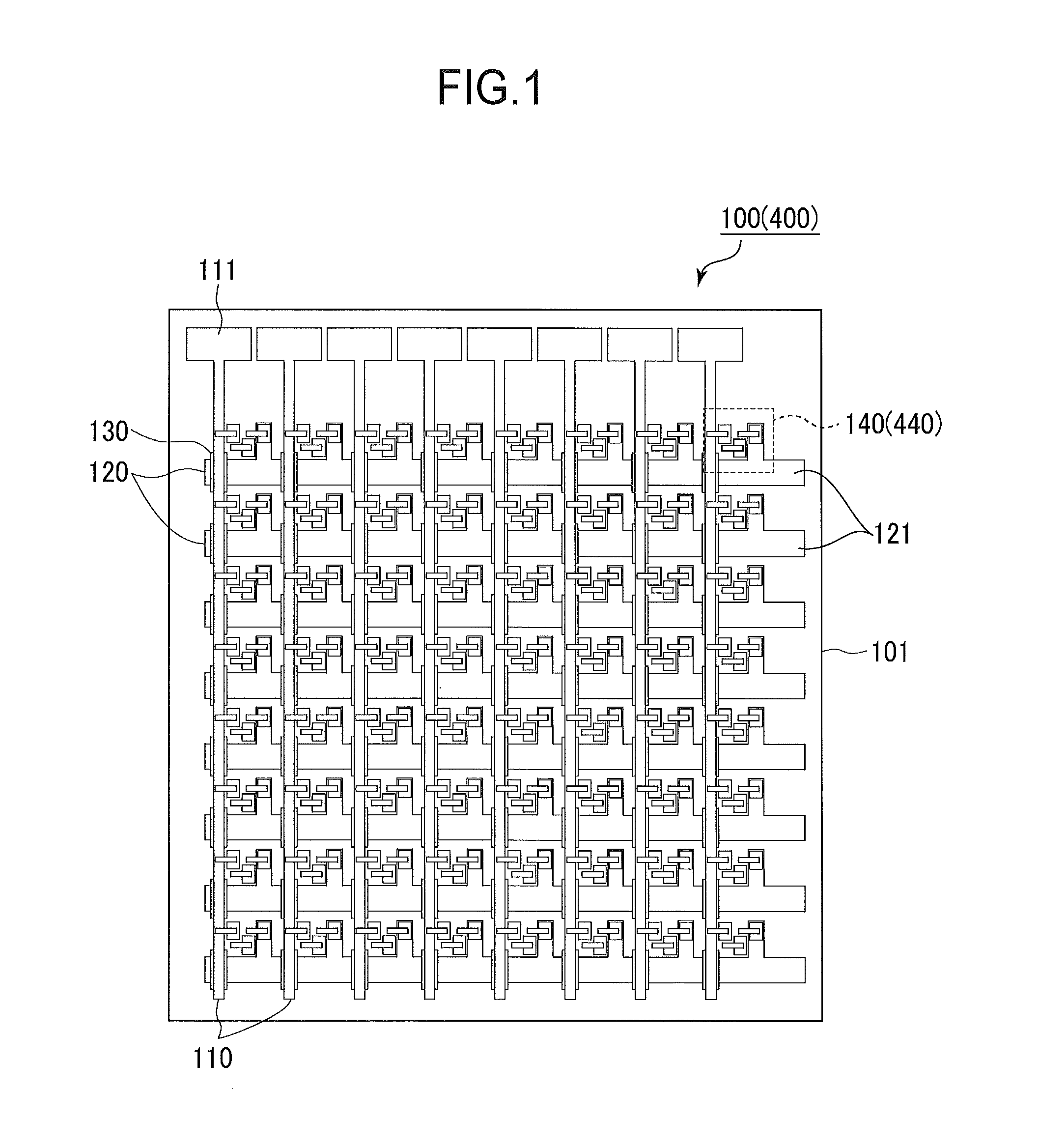
[0065]FIG. 1 is a top view illustrating the outline of a semiconductor light emitting apparatus 100. The semiconductor light emitting apparatus 100 includes a substrate 101, a plurality of first electrode wirings 110 that extend vertically, a plurality of second electrode wirings 120 that extend horizontally, and a plurality of light emitting sections 140. Reference numerals in parentheses denote those in a second embodiment.

[0066]An integrated circuit is fabricated on the substrate 101 formed of, for example, glass or plastics. Alternatively, the substrate 101 may take the form of an electrically conductive substrate such as an Si substrate or a metal substrate that is coated with an inorganic insulating film such as SiO2, SiN or Al2O3 or an organic insulating film such as epoxy, nobolak, or polyimide, thereby insulating the surface of the substrate 101.

[0067]The first electrode wirings 110 are formed by depositing a metal material, whose major composition is, for example, Au or Al...

second embodiment

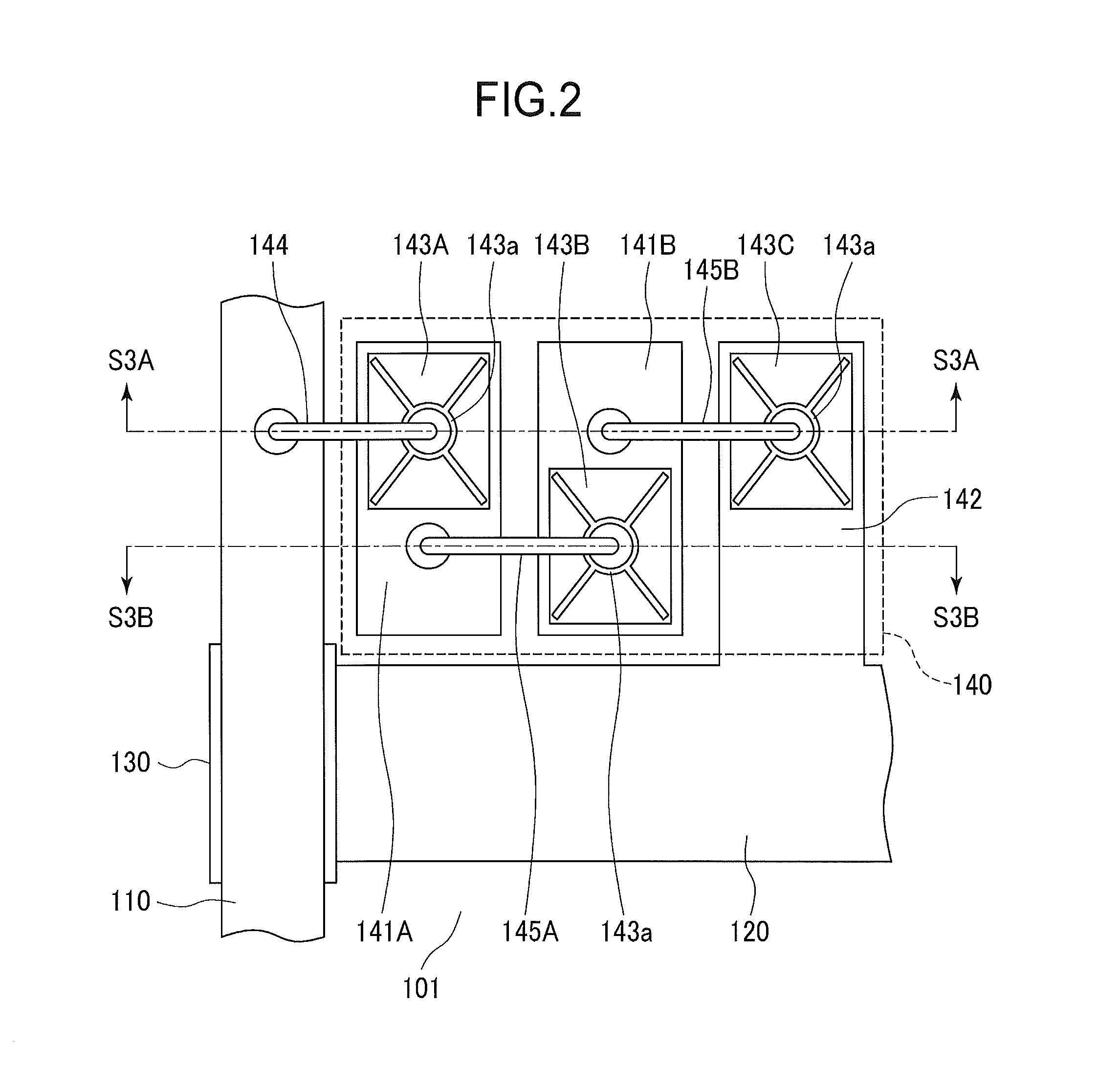
[0101]Referring back to FIG. 1, the semiconductor light emitting apparatus 400 according to a second embodiment includes a substrate 101, a plurality of first electrode wirings 110 extending in a column direction, a plurality of second electrode wirings 120 extending in a row direction, and a plurality of light emitting sections 440 arranged in a matrix. The second embodiment differs in the configuration of the light emitting sections 440 from the first embodiment.

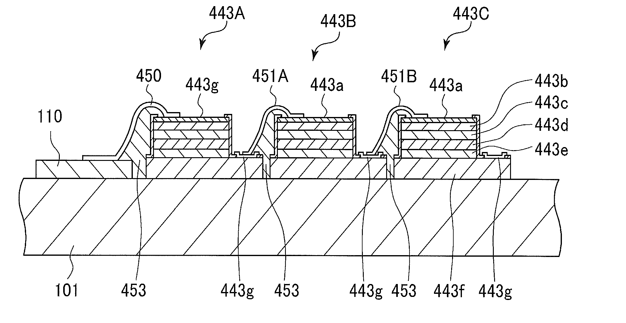
[0102]FIG. 9 is a top view illustrating the outline of the light emitting section 440 according to the second embodiment. The light emitting section 440 includes thin film LEDs 443A-443C, a first junction wiring 450, second junction wirings 451A and 451B, and a third junction wiring 452. FIG. 10 is a cross-sectional view taken along a line S10-S10 in FIG. 9.

[0103]The first junction wiring 450 serves as a first connection that connects the first electrode wiring 110 to the thin film LED 443A at the most upstream end with re...

third embodiment

[0111]FIG. 11 is a top view illustrating the outline of the configuration of an image displaying apparatus 500 according to a third embodiment. The image displaying apparatus 500 includes the semiconductor light emitting apparatus 100 according to the first embodiment, a driver apparatus 550 that drives the light emitting apparatus 100 to display an image, and a power supply 551.

[0112]The driver apparatus 550 supplies a signal voltage to one of the first electrode wiring pads 111 connected to an LED or pixel to be energized, and connects a corresponding one of the second electrode wiring pads 121 to the ground, thereby causing the LED to emit light. The driver apparatus 550 supplies the signal voltage to all of the first electrode wiring pads 111 in sequence so that the corresponding LEDs are energized in sequence, thereby scanning the row of the LEDs sequentially to form an image for one line. Likewise, the driver apparatus 550 supplies the signal voltage to all of the first electr...


PUM


Abstract

A semiconductor light emitting apparatus includes a substrate. A plurality of first electrode wirings are formed on the surface of the substrate. At least one second electrode wiring is formed on the surface of the substrate. A light emitting section is connected between a corresponding one of the plurality of first electrode wirings and the at least one second electrode wiring. The light emitting section includes a plurality of light emitting elements.

Description

BACKGROUND OF THE INVENTION[0001]1. Field of the Invention[0002]The present invention relates to a semiconductor light emitting apparatus, an image displaying apparatus, a mobile terminal, a head-up display apparatus, an image projector, ahead mounted display apparatus, and an image forming apparatus.[0003]2. Description of the Related Art[0004]An existing semiconductor light emitting apparatus employs a plurality of light emitting diodes (LEDs) arranged in a one dimensional matrix or a two-dimensional matrix, each LED functioning as a minimum unit of an image, i.e., pixel. For example, the LEDs are integrated on a substrate, and are connected to wirings as first common electrodes and wirings as second common electrodes formed on the substrate. Each chip of LED is at a corresponding pixel position. One way of increasing light power of these LEDs is to increase the amount of injected current. However, larger currents flowing through the LEDs and the first and second wirings will seri...

Claims


Application Information

Patent Timeline
IPC IPC(8): H01L33/36
CPCH01L33/36H01L25/0753H01L2224/48091H01L2224/48137H01L2224/48464H01L33/62H01L2224/73265H01L2924/00014H01L2924/00H01L2224/32257H01L24/24H01L2224/32245H01L2224/48247H01L2224/48257H01L2924/181H01L2924/00012
Inventor SUZUKI, TAKAHITOKANETO, TAISHITANAKA, SATOSHITANIGAWA, KENICHI
Owner OKI ELECTRIC IND CO LTD
Why Eureka
Try Eureka