Nonvolatile memory device, method for operating the same, and method for fabricating the same

a non-volatile memory and method technology, applied in the direction of digital storage, semiconductor/solid-state device details, instruments, etc., can solve the problems of difficult control of erase schemes using gidl current, impossible, and difficult to perform erase operations of f-n tunneling types as in the conventional art, so as to reduce the resistance of a source line, improve the degree of integration, and perform the effect of easy and efficient erase operations

Active Publication Date: 2013-08-22
SK HYNIX INC
View PDF6 Cites 42 Cited by
  • Summary
  • Abstract
  • Description
  • Claims
  • Application Information

AI Technical Summary

Benefits of technology

[0012]Embodiments of the present invention are directed to a nonvolatile memory device including vertically stacking memory cells, which can easily and efficiently perform an erase operation, reduce the resistance of a source line and increase the degree of integration, and a method for fabricating the same.

Problems solved by technology

However, because channels are separated from the body of a substrate in the Pipe-shaped BiCS (PBiCS) structure, an erase operation of an F-N tunneling type as in the conventional art, which injects holes into the floating gates of memory cells by applying a high voltage to the body of the substrate, becomes impossible.
Nevertheless, such an erase scheme using GIDL current is difficult to control.

Method used


Image

  • Nonvolatile memory device, method for operating the same, and method for fabricating the same
  • Nonvolatile memory device, method for operating the same, and method for fabricating the same
  • Nonvolatile memory device, method for operating the same, and method for fabricating the same

Examples


first embodiment

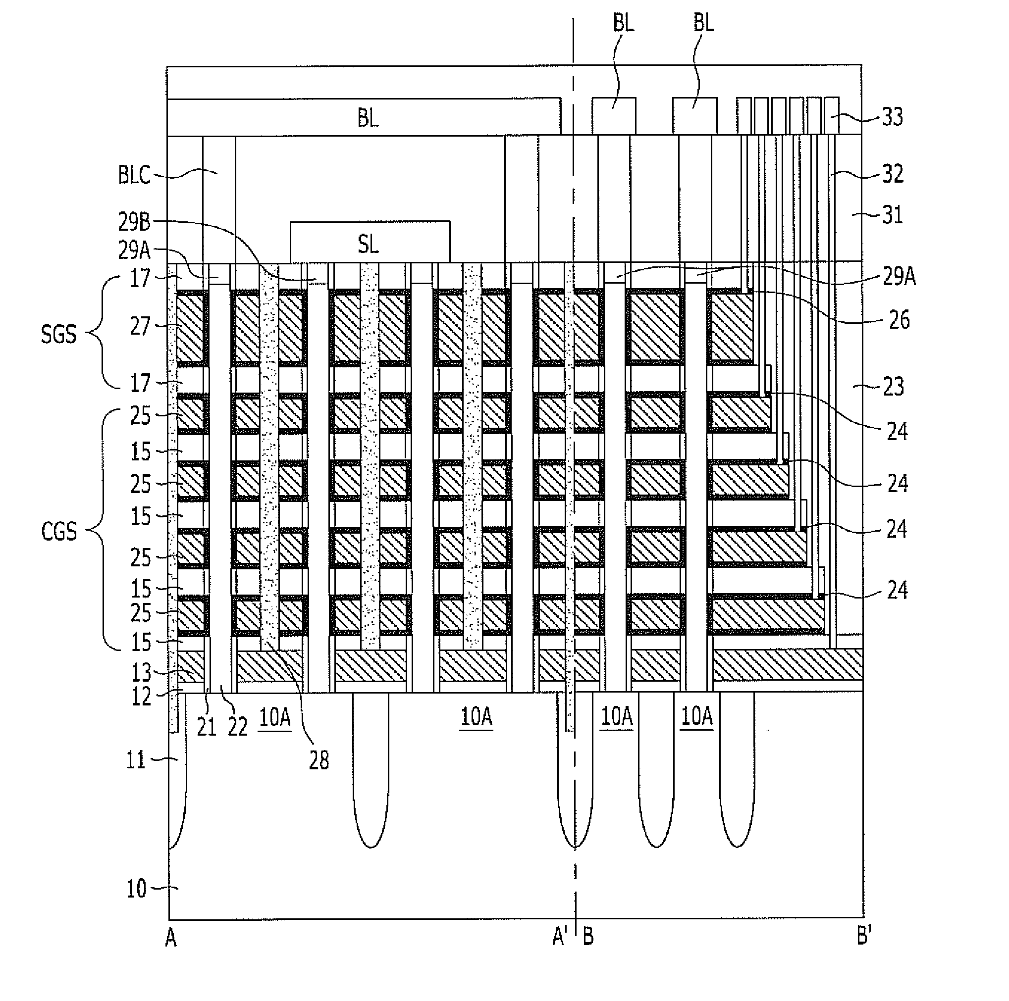
[0031]Hereafter, a nonvolatile memory device in accordance with the present invention, a method for operating the same and a method for fabricating the same will be described with reference to FIGS. 1 to 13.

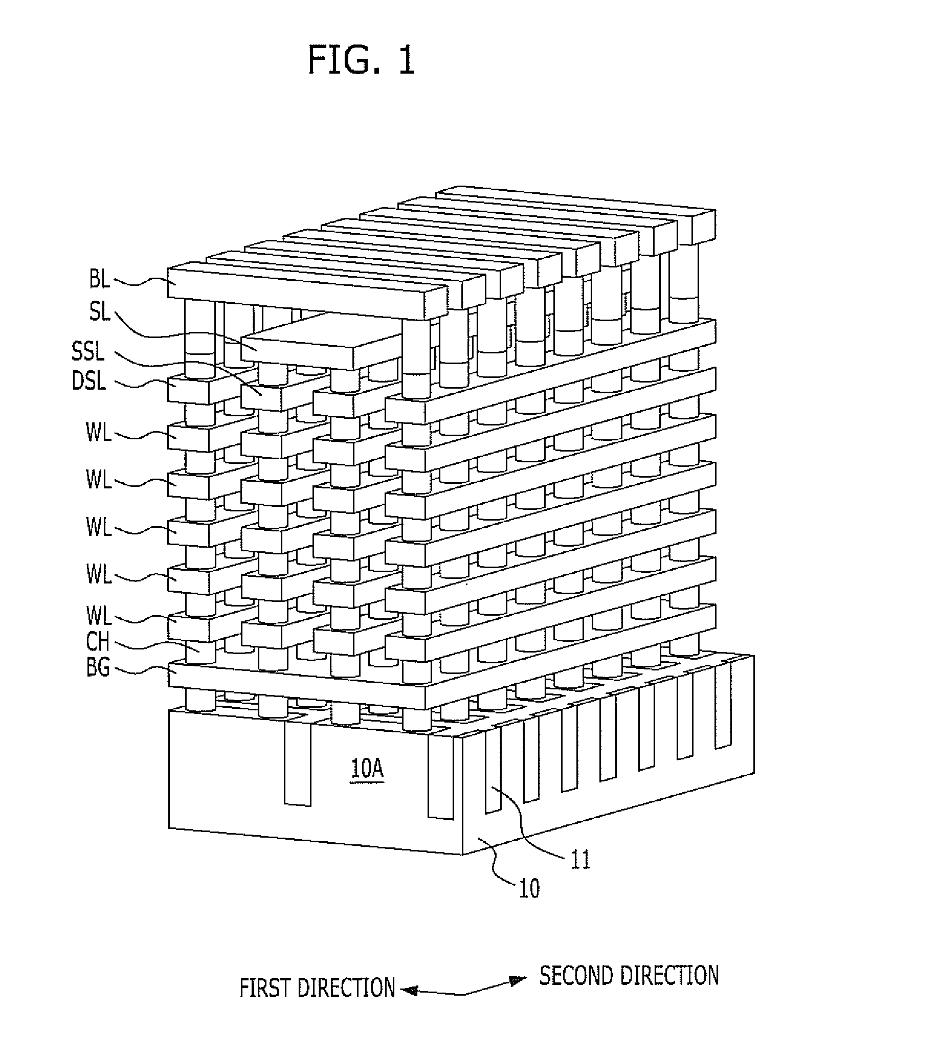
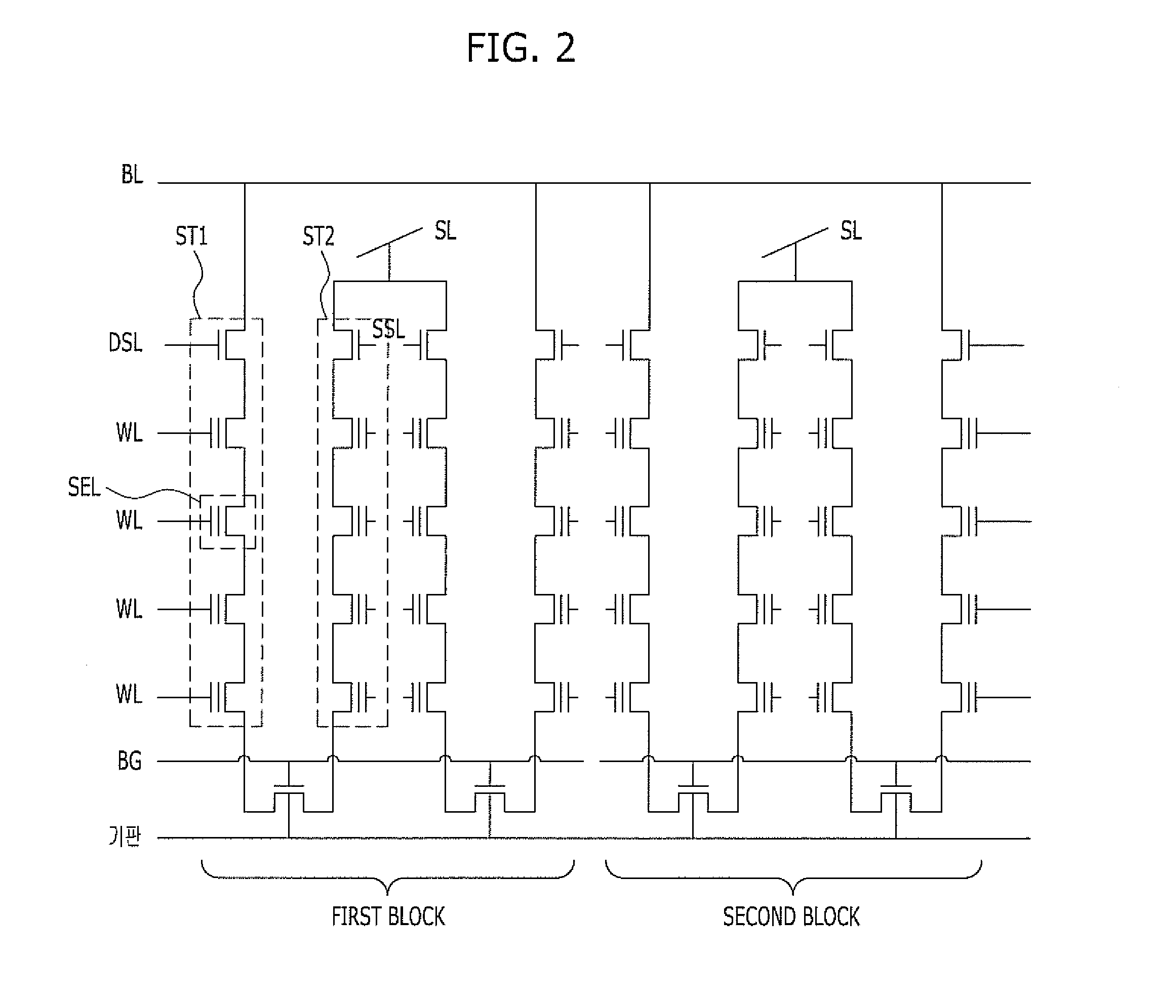
[0032]FIGS. 1 and 2 are respectively a perspective view and a circuit diagram showing a nonvolatile memory device in accordance with a first embodiment of the present invention. While only one block is shown in FIG. 1 and two blocks adjacent in a first direction are shown in FIG. 2 for the sake of convenience in explanation, it is to be noted that a nonvolatile memory device includes a plurality of blocks which are arranged in the first direction and a second direction.

[0033]Referring to FIGS. 1 and 2, the nonvolatile memory device according to the present embodiment includes a substrate 10, a pair of vertical strings ST1 and ST2, and a bottom gate BG. The substrate 10 may include a P-type semiconductor. A plurality of active regions 10A is defined in the substrate 10 by an isola...

third embodiment

[0105]FIGS. 17 and 18 are views explaining a nonvolatile memory device in accordance with the present invention, a method for fabricating the same and a method for operating the same. FIG. 17 is shown on the basis of the same assumptions as the cross-sectional view of FIG. 10. FIG. 18 is shown on the basis of the same assumptions as FIG. 2.

[0106]Referring to FIGS. 17 and 18, the nonvolatile memory device according to the present embodiment includes a substrate 10, which is constituted by a P-type semiconductor and has a plurality of active regions 10A defined by an isolation layer 11, and a pair of vertical strings ST1 and ST2 which are formed on each active region 10A. In particular, connection of vertical strings ST1 and ST2 is controlled in such a manner that a lowermost word line 25 forms an inverted region in the active region 10A. Namely, the device according to this third embodiment has a structure excluding the bottom gate BG, the underlying gate dielectric layer, and the ov...

fourth embodiment

[0111]FIG. 19 is a view explaining a nonvolatile memory device in accordance with the present invention, a method for fabricating the same and a method for operating the same. FIG. 19 is shown on the basis of the same assumptions as FIG. 13. The circuit diagram of the present embodiment is substantially the same as FIG. 18.

[0112]Referring to FIG. 19, the nonvolatile memory device according to the present embodiment includes a substrate 10, which is constituted by a P-type semiconductor and has a plurality of active regions 10A defined by an isolation layer 11, and a pair of vertical strings ST1 and ST2 which are formed on each active region 10A. In particular, the connection of vertical strings ST1 and ST2 is controlled in such a manner that a lowermost word line 36 forms an inverted region in the active region 10A.

[0113]In other words, the device according to the fourth embodiment has a structure in which the bottom gate BG and the overlying interlayer dielectric layer are omitted ...


PUM


Abstract

A nonvolatile memory device includes a substrate including a plurality of active regions which are constituted by a P-type semiconductor; first and second vertical strings disposed over each active region, wherein each of the first and second strings includes a channel vertically extending from the substrate, a plurality of memory cells, and a select transistor, wherein the plurality of memory cells and the select transistor are located along the channel; and a bottom gate being interposed between a lowermost memory cell and the substrate, contacting the channel with a first gate dielectric layer interposed therebetween, and controlling connection of the first vertical string with the second vertical string.

Description

CROSS-REFERENCE TO RELATED APPLICATIONS[0001]The present application claims priority of Korean Patent Application No. 10-2012-0016986, filed on Feb. 20, 2012, which is incorporated herein by reference in its entirety.BACKGROUND[0002]1. Field[0003]Exemplary embodiments of the present invention relate to a nonvolatile memory device, a method for operating the same and a method for fabricating the same, and more particularly, to a nonvolatile memory device which includes a plurality of memory cells vertically stacked from a substrate, a method for operating the same and a method for fabricating the same.[0004]2. Description of the Related Art[0005]A nonvolatile memory device is a memory device which maintains stored data as they are even when power supply is interrupted. Currently, various nonvolatile memory devices, for example, a NAND type flash memory and the like are widely used.[0006]Recently, as improving the degree of integration of a two-dimensional nonvolatile memory device in...

Claims


Application Information

Patent Timeline
Patent Type & Authority Applications(United States)
IPC IPC(8): G11C16/04H01L21/336H01L29/78
CPCG11C16/0425H01L27/11582H01L2924/0002H10B43/50H10B43/35H10B43/27H01L2924/00H01L27/0688H01L29/7926H10B43/20G11C16/0483G11C5/02G11C5/06G11C16/04H10B41/27H10B41/35H10B41/41H10B43/40H10B99/00G11C16/14G11C16/26H01L21/30604H01L21/768H01L23/528
Inventor OH, SEUL-KILEE, JUN-HYUK
Owner SK HYNIX INC
Why Eureka
Try Eureka