

Plasma boundary limiter unit and apparatus for treating substrate
a boundary limiter unit and substrate technology, applied in mechanical equipment, basic electric elements, coatings, etc., can solve the problems of affecting the movement path of confinement rings, difficult to control the plasma density of each region in inner regions of confinement rings, and low plasma leakage prevention
- Summary
- Abstract
- Description
- Claims
- Application Information
AI Technical Summary
Benefits of technology
Problems solved by technology
Method used
Image

Examples
Embodiment Construction
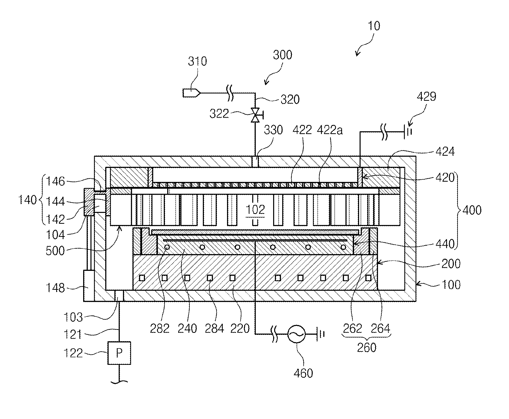
[0039]Hereinafter, a substrate treating apparatus according to exemplary embodiments of the present invention will be described in detail with reference to the accompanying drawings. In description of the present invention, detailed descriptions related to well-known functions or configurations will be ruled out in order not to unnecessarily obscure subject matters of the present invention.
[0040]FIG. 1 is a view of a substrate processing apparatus 10 according to an embodiment of the present invention. The substrate treatment apparatus 10 treats a substrate W by using plasma. In the current embodiment of the present invention, an apparatus for treating a substrate W by using plasma will be described as an example. However, technical features of the present invention are not limited thereto.
[0041]For example, the technical features of the present invention may be applied to various kinds of apparatuses which are capable of treating the substrate W by using plasma.
[0042]Referring to F...
PUM
| Property | Measurement | Unit |
|---|---|---|
| circumference | aaaaa | aaaaa |
| distance | aaaaa | aaaaa |
| thickness | aaaaa | aaaaa |
Abstract
Description
Claims
Application Information