Method and Circuitry for Matching Impedance
a technology of impedance matching and circuitry, applied in the field of analog interface technology of communication equipment, can solve the problems of inflexible product configuration and management, increased design cost, and difficulty in impedance matching of wireless access boxes and telephones, and achieve the effects of simple implementation technology, low cost and reliable operation
- Summary
- Abstract
- Description
- Claims
- Application Information
AI Technical Summary
Benefits of technology
Problems solved by technology
Method used
Image
Examples
first application example
The First Application Example
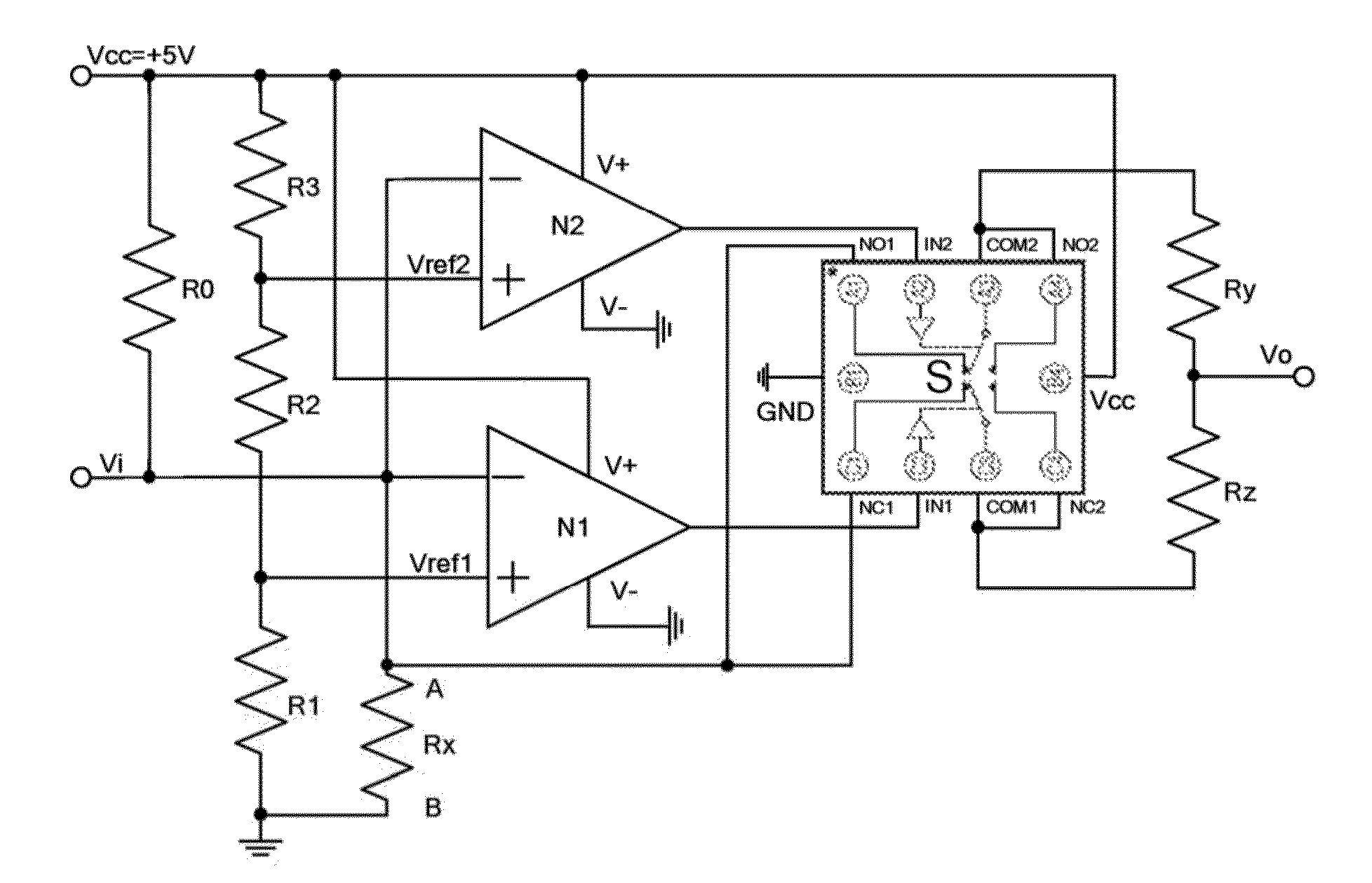
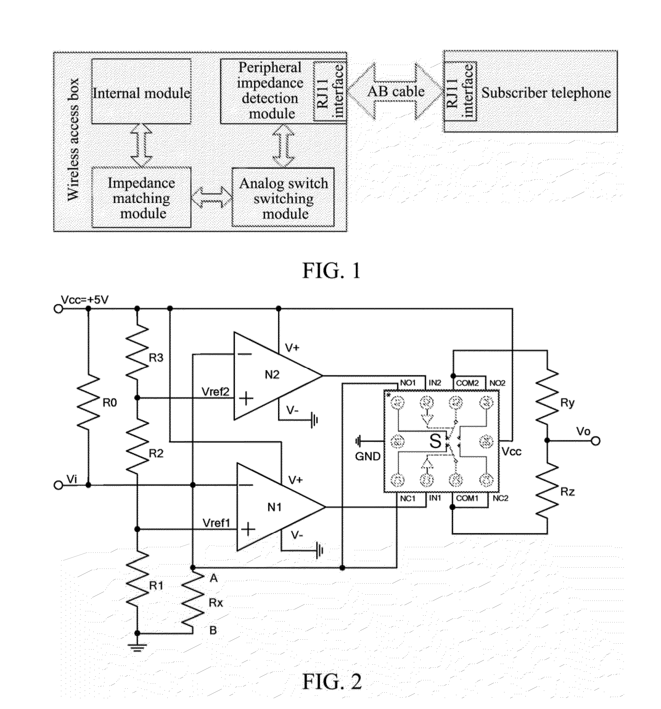
[0046]FIG. 2 shows an impedance matching circuit of a wireless access box interface in accordance with the first application example of the present invention, wherein,
[0047]the ADC detection module comprises the resistor R0, the resistor R1, the resistor R2, the resistor R3, the voltage comparator N1 and the voltage comparator N2, wherein, one end of the resistor R0 is connected to the power supply Vcc, the other end is connected to the impedance Rx of the subscriber telephone, as well as the negative input ends of the voltage comparator N1 and the voltage comparator N2; one end of the resistor R1 is connected to the ground, and the other end is connected to the positive input end of the voltage comparator of N1 and the resistor R2; one end of the resistor R2 is connected to the positive input end of the voltage comparator N1 and the resistor R1, and the other end is connected to the positive input end of the voltage comparator N2 and the resistor R3; on...
second application example
The Second Application Example
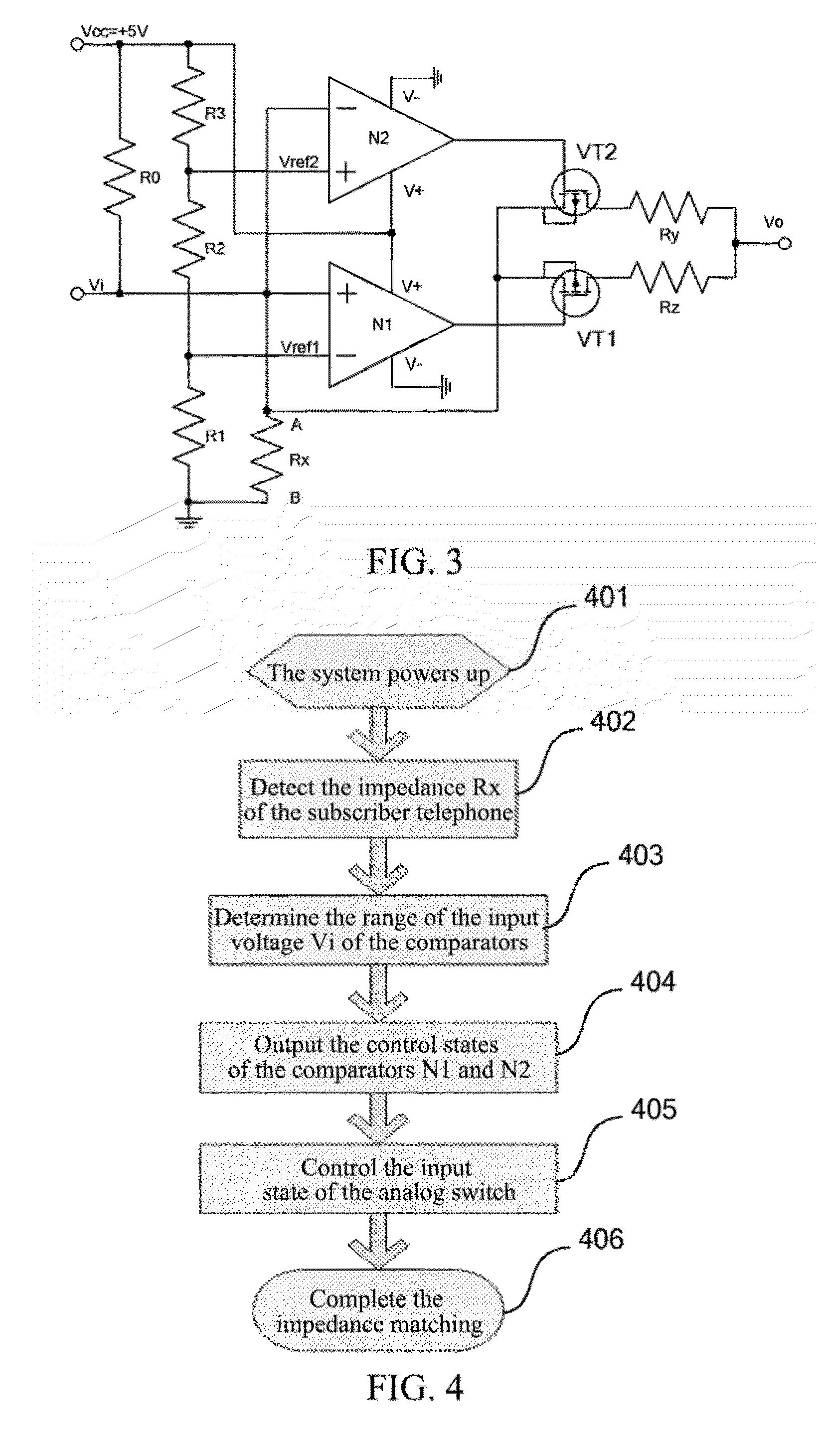
[0056]FIG. 3 shows an impedance matching circuit of the wireless access box interface in accordance with the second application example of the present invention, wherein, the peripheral impedance detection module and the impedance matching module are the same as their peers in the first application example, the analog switch switching module consists of two field effect transistors VT1 and VT2 which are P-channel CMOS type, wherein, the grid of the FET VT1 is connected to the output end of the voltage comparator N1, the grid of the FET VT2 is connected to the output end of the voltage comparator N2, and the drains of the FETs VT1 and VT2 are connected to the end of the impedance Rx of the subscriber telephone that is not connected to the ground, the source of the FET VT1 is connected to one end of the resistor Ry, and the source of the FET VT2 is connected to one end of the resistor Rz.
[0057]The same path of signal voltage is input in the two voltage co...
PUM
 Abstract
Description
Claims
Application Information


