Radioactive ray detector card

a detector card and radioactive ray technology, applied in the direction of radiation intensity measurement, instruments, x/gamma/cosmic radiation measurement, etc., can solve the problem of easy complex wiring structure of radioactive ray detecting units, and achieve the effect of simplifying the wiring structure of signal lines, avoiding dead space generation, and increasing detection sensitivity

Inactive Publication Date: 2013-09-26
HITACHI LTD
View PDF2 Cites 4 Cited by
  • Summary
  • Abstract
  • Description
  • Claims
  • Application Information

AI Technical Summary

Benefits of technology

[0004]In a radioactive ray detecting apparatus described in the Patent Document 1 is provided a radioactive ray detecting unit, which is constructed with plural numbers of semiconductor radioactive ray detectors on the side of a detecting surface of a socket board mounting substrate, and is provided a measuring circuit unit for processing a radioactive ray detection signal on the opposite side of the socket board mounting substrate. According to the Patent Document 1, it is said, since that semiconductor radioactive ray detector is simplified in the wiring structure of signal lines in the periphery of the detector, it is possible to avoid a dead space generating due to the signal lines in the periphery of the detector when plural numbers of detectors are combined. As a result of this, it is said, plural numbers of the semiconductor radioactive ray detectors can be provided be dense or crowded, and thereby increasing the sensitivity of detection, as well as, enabling to remove unevenness due to joints. However, the semiconductor radioactive ray detecting apparatus according to the Patent Document 1, the wiring structure within the radioactive ray detecting unit can be easily complex; therefore, a further improvement of the wiring structure from an viewpoint of easiness of manufacturing comes up to be a problem to be dissolved.
[0013]According to the present invention, it is possible to provide a radioactive ray detector card, for enabling to simplify the wiring structure between that plural numbers of semiconductor elements and electronics parts to be connected therewith, in an inside of the radioactive ray detector equipped with the plural numbers of semiconductor elements.

Problems solved by technology

However, the semiconductor radioactive ray detecting apparatus according to the Patent Document 1, the wiring structure within the radioactive ray detecting unit can be easily complex; therefore, a further improvement of the wiring structure from an viewpoint of easiness of manufacturing comes up to be a problem to be dissolved.

Method used


Image

  • Radioactive ray detector card
  • Radioactive ray detector card
  • Radioactive ray detector card

Examples


Embodiment Construction

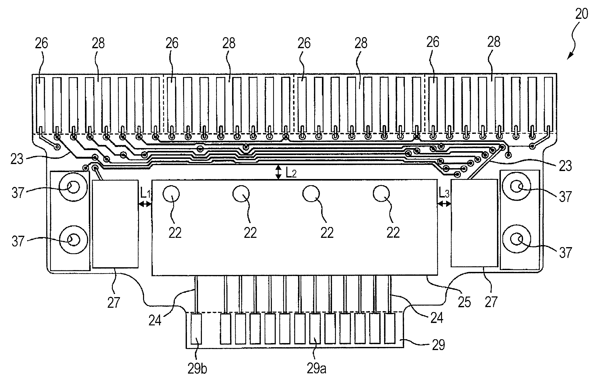
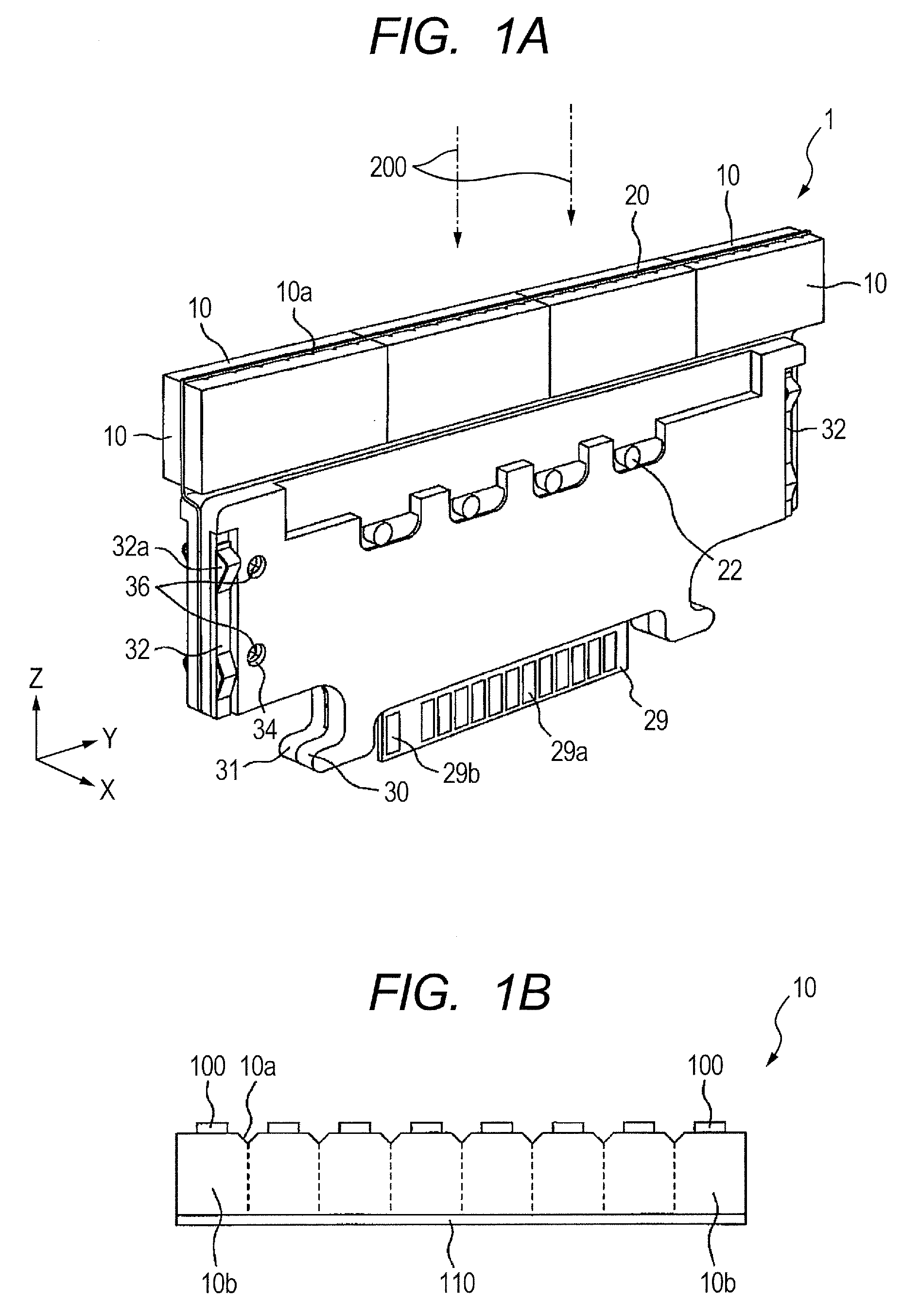
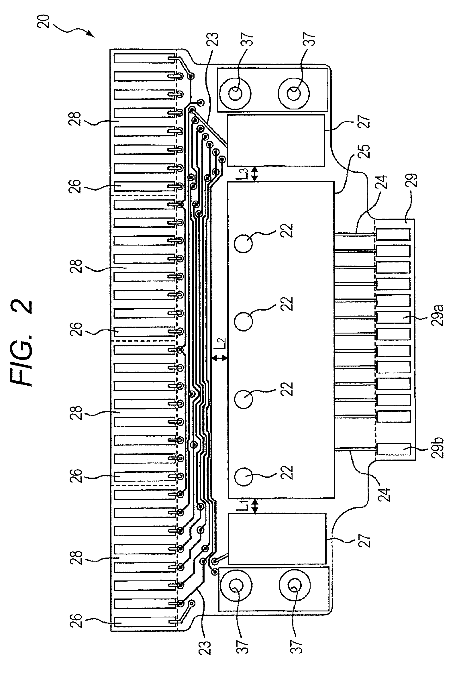
Outlook of Structure of Radioactive Ray Detector Card 1

[0021]FIG. 1 is a diagrammatic perspective view for showing an example of a radioactive ray detector card, according to an embodiment of the present invention. The radioactive ray detector card 1 according to the present embodiment has a card-type configuration, and is a radioactive ray detector card for detecting radioactive rays 200, such as, the gamma (γ) rays, the X rays, etc. As is shown in FIG. 1A, the radioactive rays 200 propagate directing from an upper portion towards a lower portion in the figure. In other words, the radioactive rays 200 advance along with the direction directing from a semiconductor element 10 of the radioactive ray detector card 1 to card holders 30 and 31, and thereby reaching onto the radioactive ray detector card 1. And, the radioactive rays 200 are incident upon a side surface of the semiconductor element 10 of the radioactive ray detector card 1 (i.e., the surface facing to the above in FIG. 1A...


PUM


Abstract

A radioactive ray detector card comprises semiconductor elements on a substrate, each having a plurality of first electrodes, provided on one of main surfaces thereof, and a second electrode, provided on other of main surfaces thereof; the substrate having first electrode wirings electrically connected with the plurality of first electrodes, and card edge portions, which transmit signals from the plurality of semiconductor elements to an external electric circuit; the second electrode corresponding to a second electrode identifier, for identifying the semiconductor elements; the first electrodes corresponding to first electrode identifiers, for identifying the plurality of first electrodes, respectively; and the first electrode wirings electrically connect between the first electrodes, corresponding to one of the first electrode identifiers on one semiconductor element of the plurality of semiconductor elements, and the first electrodes, corresponding to one of the same first electrode identifiers on the other semiconductor element.

Description

TECHNICAL FIELD[0001]The present invention relates to a radioactive ray detector card. In particular, the present invention relates to a radioactive ray detector card for detecting radiations of gamma (γ) rays, X rays, etc.BACKGROUND OF THE INVENTION[0002]As a conventional radioactive ray detector is already known, in the following Patent Document 1, for example, a semiconductor radioactive ray detector, comprising a semiconductor element, an anode electrode attached on one surface of said semiconductor element, a cathode electrode attached on the other surface of said semiconductor element, and a signal line, one end thereof being connected with at least one of the anode electrode and the cathode electrode and the other end thereof extending straight from said electrode thereby to output a signal from that electrode.PRIOR ART DOCUMENTSPatent Documents[0003][Patent Document 1] Japanese Patent Laying-Open No. 2005-109269 (2005).BRIEF SUMMARY OF THE INVENTIONProblem(s) to be Dissolved...

Claims


Application Information

Patent Timeline
Patent Type & Authority Applications(United States)
IPC IPC(8): G01T1/24
CPCG01T1/243G01T1/24
Inventor KAWAUCHI, HIDETAKASUNAGA, YOSHINORITAKAHASHI, ISAO
Owner HITACHI LTD
Why Eureka
Try Eureka