Liquid Crystal Display Device and Driving Method

Inactive Publication Date: 2013-09-26
TCL CHINA STAR OPTOELECTRONICS TECH CO LTD
View PDF5 Cites 12 Cited by
  • Summary
  • Abstract
  • Description
  • Claims
  • Application Information

AI Technical Summary

Benefits of technology

[0024]The efficacy of the present invention is that to be distinguished from the known techniques, according to the present invention, when a scan signal is received through the switching unit, the first voltage source supplies a first voltage to the pixel unit, and when the switching unit receives no scan signal, the second voltage source supplies a second voltage

Problems solved by technology

As a consequence, for a low grey scale image, the left and right side edges of the liquid crystal display panel show re

Method used


Image

  • Liquid Crystal Display Device and Driving Method
  • Liquid Crystal Display Device and Driving Method
  • Liquid Crystal Display Device and Driving Method

Examples


Embodiment Construction

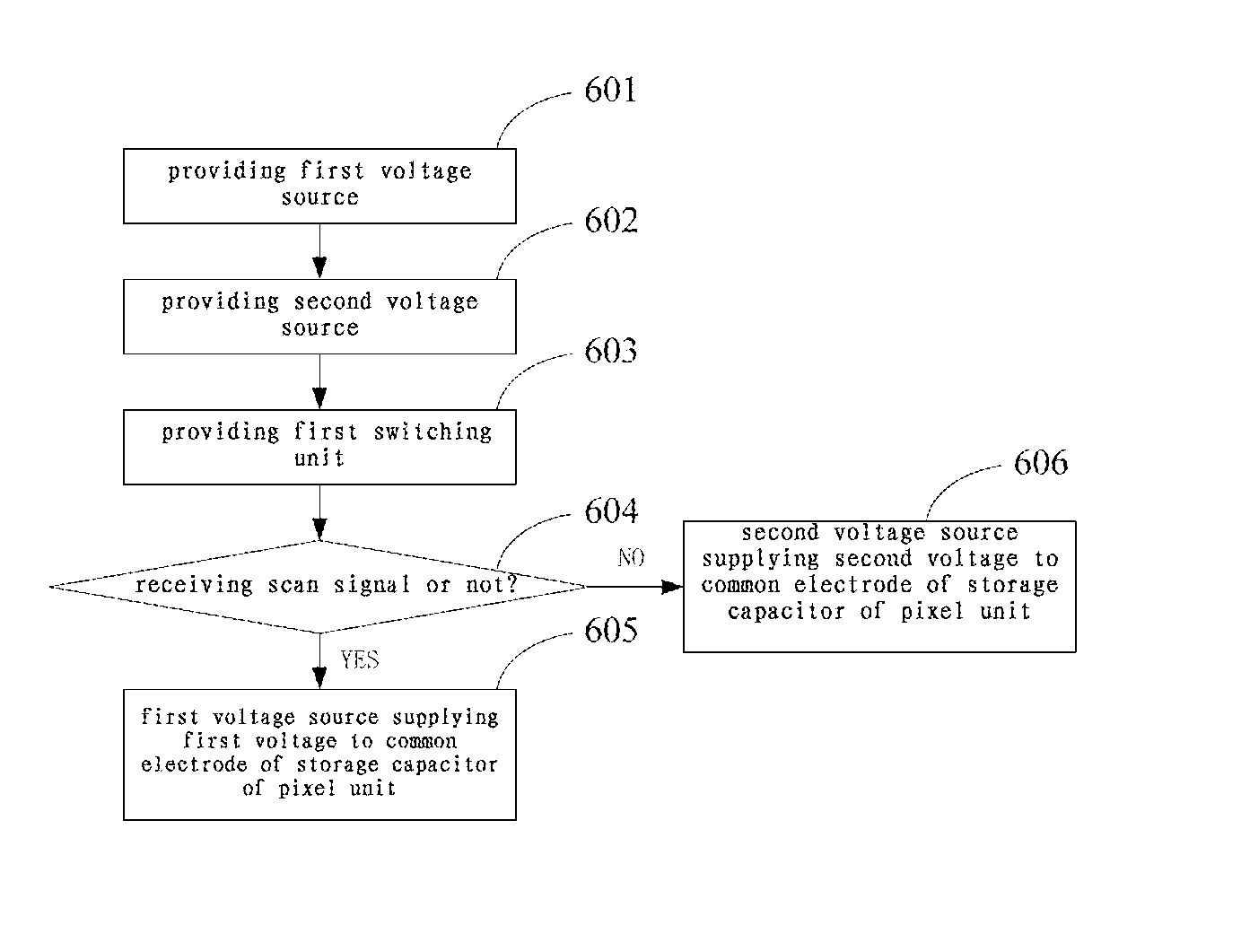
[0032]A detailed description will be given hereinafter with reference to the accompanying drawings and embodiments.

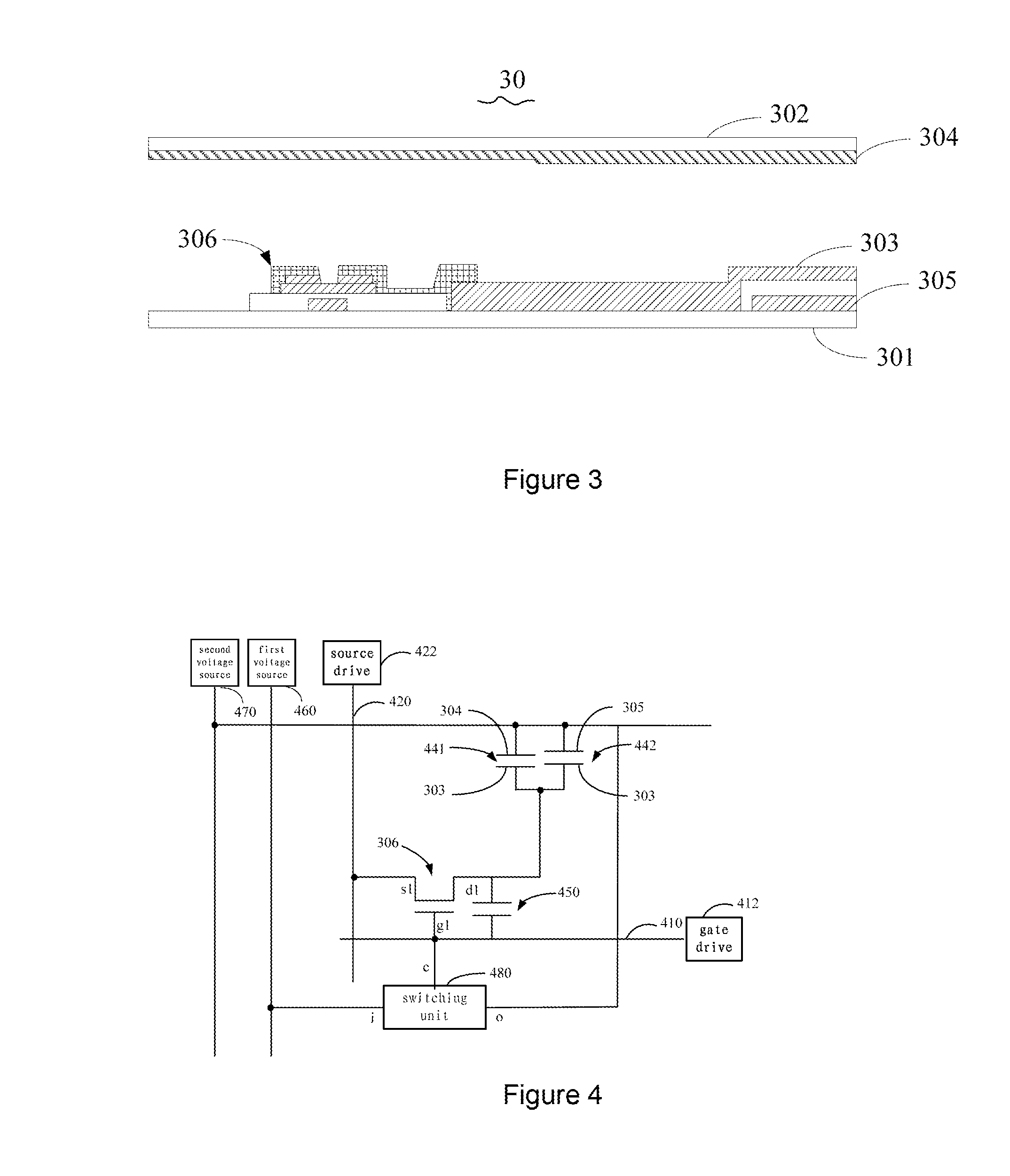
[0033]The present invention aims to provide a liquid crystal display device, which comprises a plurality of pixel units arranged in an array. As shown in FIG. 3, each pixel unit 30 comprises a first substrate 301 and a second substrate 302 that are arranged opposite to each other and a liquid crystal layer (not shown) interposed between the first substrate 301 and the second substrate 302. In the embodiment, the first substrate 301 is a TFT (Thin Film Transistor) substrate and the second substrate 302 is a CF (Color Filter) substrate.

[0034]FIG. 4 is diagram showing a driving circuit of the liquid crystal display device according to the present invention. Referring to both FIGS. 3 and 4, taking a single pixel unit as an example, in the instant embodiment, the driving circuit of the liquid crystal display device comprises: a scan line 410, a data line 420, a first TFT 306...


PUM


Abstract

A liquid crystal display device includes a first voltage source providing a first voltage; a second voltage source providing a second voltage greater than the first voltage; and a switching unit arranged at a connection between a gate terminal of a first TFT and a scan line. The switching unit has a control terminal electrically connected to the scan line, an input terminal electrically connected to the first voltage source, and an output terminal electrically connected to the second voltage source and a common electrode of a storage capacitor of a pixel unit. When the switching unit receives a scan signal, the first voltage source supplies the first voltage to the common electrode of the storage capacitor of the pixel unit. When no scan signal is received, the second voltage source supplies the second voltage to the common electrode of the storage capacitor of the pixel unit.

Description

BACKGROUND OF THE INVENTION[0001]1. Field of the Invention[0002]The present invention relates to the field of displaying techniques, and in particular to a liquid crystal display device and a driving method thereof.[0003]2. The Related Arts[0004]A liquid crystal display device often comprises a first substrate, a second substrate, and a liquid crystal layer arranged between the first substrate and the second substrate. The liquid crystal display device comprises a plurality of pixel units, each of which comprises a pixel electrode made of indium tin oxide and formed on the first substrate and a common electrode formed on the second substrate.[0005]As shown in FIG. 1, a single pixel unit is taken as an example for illustration purposes. A known driving circuit for liquid crystal display device comprises: a scan line 110, a data line 120, a first TFT (Thin Film Transistor) 130, a liquid crystal capacitor 141, and a storage capacitor 142. The liquid crystal capacitor 141 is constituted...

Claims


Application Information

Patent Timeline
IPC IPC(8): G09G3/36G06F3/038
CPCG09G3/3648G09G2300/043G09G2300/0814G09G3/36G09G2320/0233G06F3/038G09G2320/0219
Inventor LIN, CHIA CHIANGHOU, HUNG-LUNGHE, CHENGMING
Owner TCL CHINA STAR OPTOELECTRONICS TECH CO LTD
Why Eureka
Try Eureka