LED image projection apparatus

a technology of led image and projection apparatus, which is applied in the direction of display means, instruments, advertising, etc., can solve the problems of dim and unclear image, high manufacturing cost of such a configuration, and structure defects

Inactive Publication Date: 2013-10-03
WAITRONY OPTOELECTRONICS
View PDF15 Cites 10 Cited by
  • Summary
  • Abstract
  • Description
  • Claims
  • Application Information

AI Technical Summary

Benefits of technology

[0009]The present invention addresses the above-described deficiencies and others. Specifically, the present invention provides a LED image projection apparatus that is novel, and easy and inexpensive to manufacture. To solve

Problems solved by technology

This conventional structure is lacking in that although the plastic shell installed on the exterior of the LED may project images, the manufacturing costs of such a configuration are high.
Therefore, other prior art teaches of directly printing the images on the LED, but this str

Method used


Image

  • LED image projection apparatus
  • LED image projection apparatus
  • LED image projection apparatus

Examples


Embodiment Construction

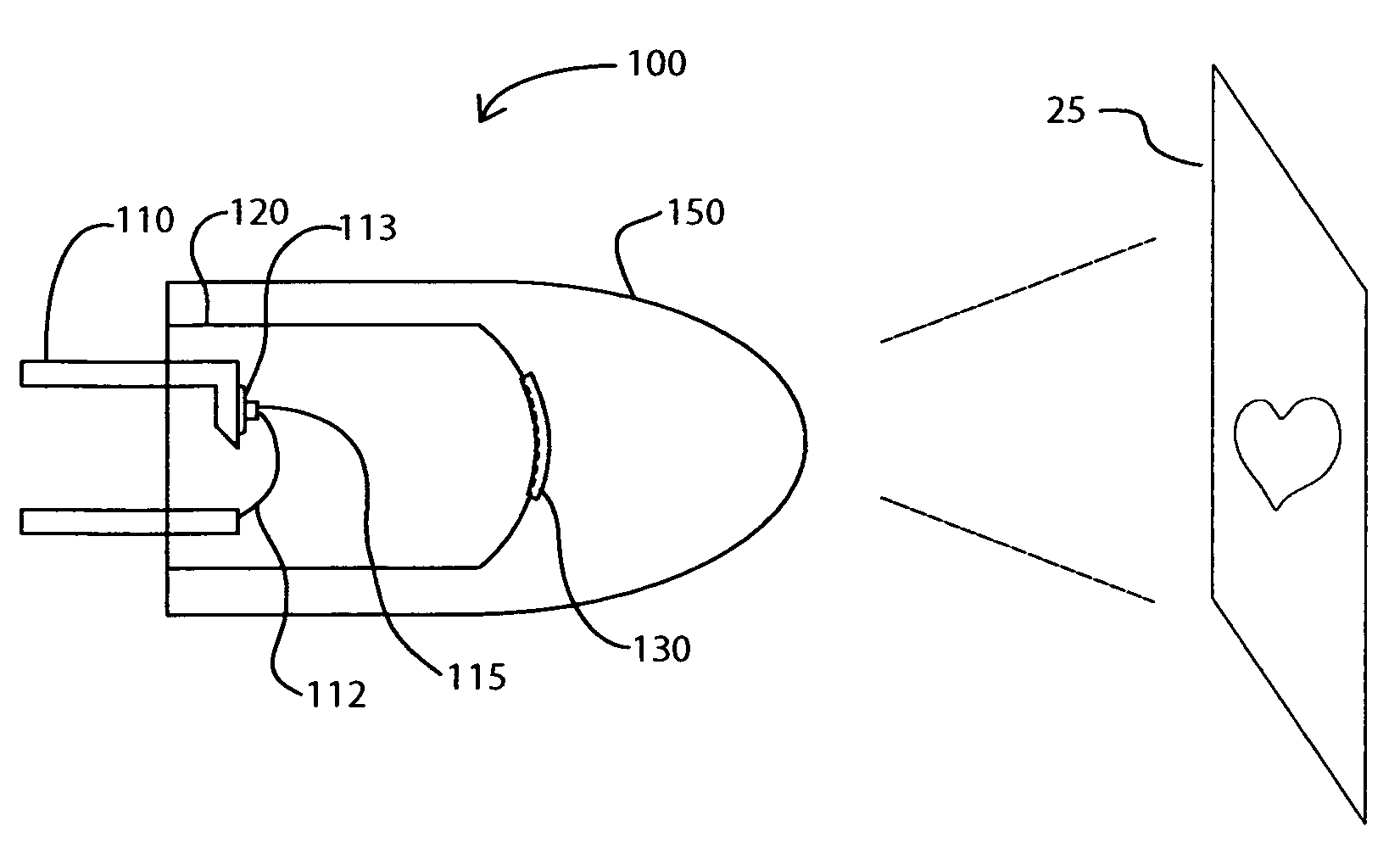
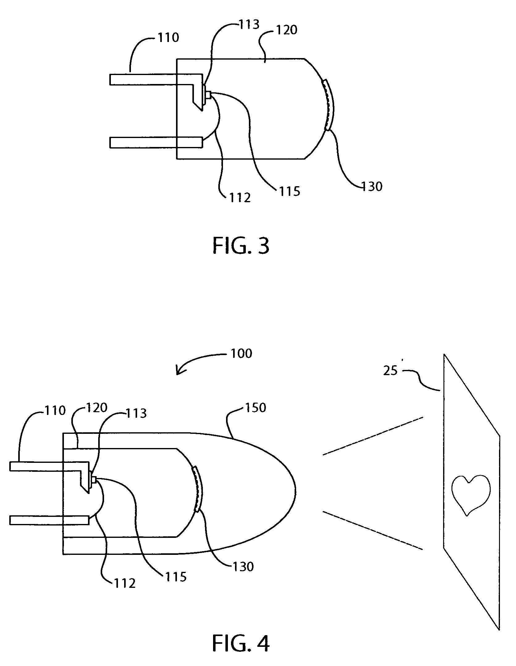
[0019]As shown in FIGS. 3 and 4, an LED image projection apparatus 100 may comprise a LED body 120 comprising a light emitting diode (LED) wafer 115 as a light source, a set of electrically coupling conductive lead frames 110, a conductive coupling wire 112, and a pattern layer 130 imprinted or impinged upon on the distal portion of the LED body 120. The wafer 115 is bonded to at least one lead frame 110 by a bonding agent 113. The pattern layer 130 may comprise an image or indicia which may include visible pictures, characters, numbers, symbols, marks, schematic views, signs, photos and drawings. The conductive coupling wire 112 may be comprised of any suitable electrically conductive material known in the art such as gold, aluminum, copper, silver, or other alloy and is at least partially contained within said LED body 120. The LED image projection apparatus 100 further comprises a transparent epoxy layer 150 which is fully encapsulated or formed about the distal portion of the LE...


PUM


Abstract

A light emitting diode image projection apparatus, comprising a light emitting diode as a light source, a transparent optical grade LED body, having a pattern layer and having an exterior epoxy layer formed about said LED body. The distal end of the LED body is a substantially flat-curved surface (while not being totally flat), while the transparent encapsulating epoxy layer is a sharp-curved, convex surface. This configuration of effective lens structures provides a double encapsulation such that structurally, the effects of the light reflection and the image projection are the same as those of the LED with external plastic outside shells, but the instant invention greatly reduces cost over the former.

Description

FIELD OF INVENTION[0001]The present disclosure relates generally to light emitting diodes (LED's) and, more particularly, to an LED image projection apparatus.BACKGROUND[0002]Light-emitting diodes (LED) may have a basic structure comprising a few components such as a light-emitting wafer, some sort of structural housing, bonding agent (such as glue), and conductive coupling wires. Bonding agents may be used as a silver epoxy or silicone epoxy, and one or more light-emitting wafer may be bonded together and coupled via conductive wires. The epoxies may form a head of some sort of resin, and may take on different encapsulation shapes, which generate different illumination appearances and different spotlighting effects. For example, a relatively flat-curved head makes the emitted light scattered, and while relatively sharp-curved head may make the emitted light more centralized.[0003]In some conventional LED image projection structures, a plastic outer shell is installed on the exterio...

Claims


Application Information

Patent Timeline
IPC IPC(8): G03B21/26
CPCG09F19/18H01L33/58G09F2013/222H01L2924/181H01L2224/48091H01L2224/48247H01L2924/00012H01L2924/00014
Inventor HING-WAI, KHOK
Owner WAITRONY OPTOELECTRONICS
Why Eureka
Try Eureka