

Method implemented in a computer for the numerical simulation of semiconductor devices containing tunnel junctions
- Summary
- Abstract
- Description
- Claims
- Application Information
AI Technical Summary
Benefits of technology
Problems solved by technology
Method used
Image

Examples
Embodiment Construction
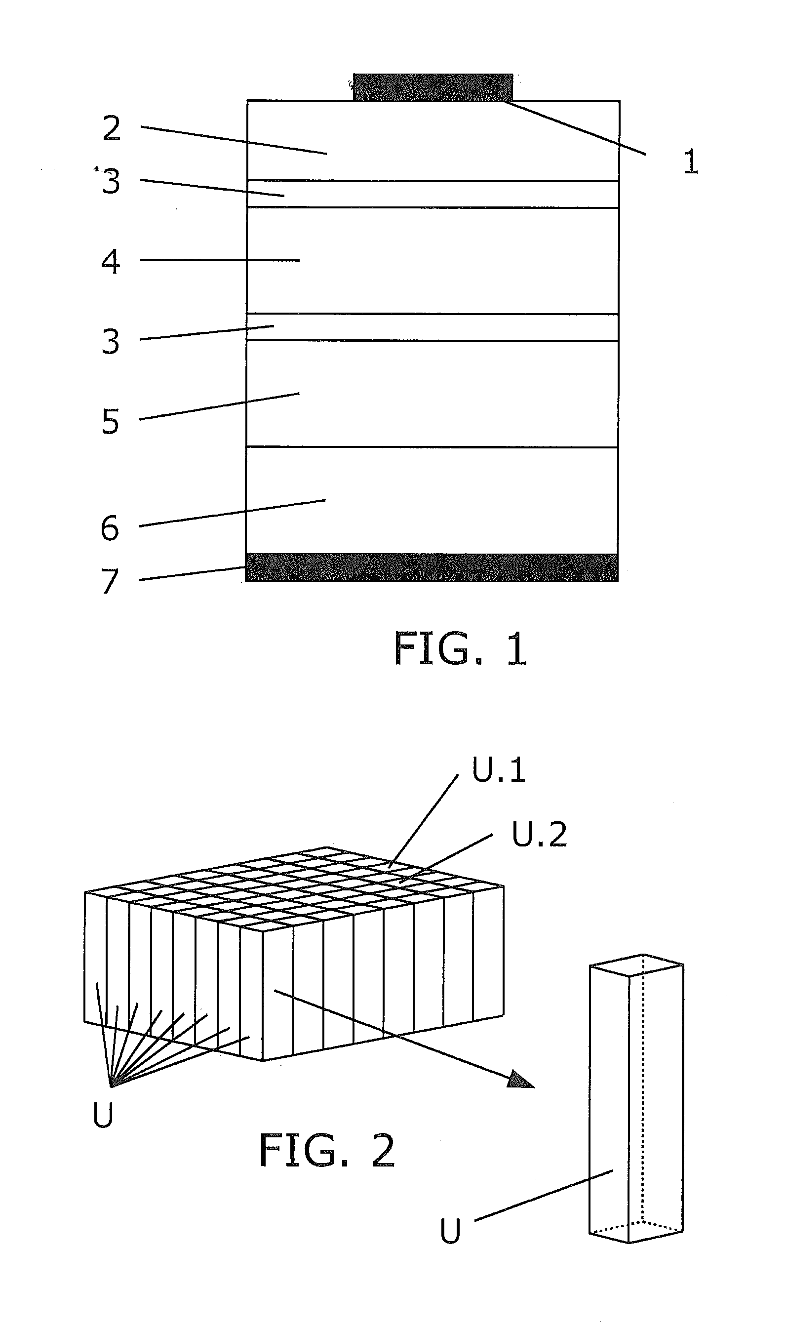
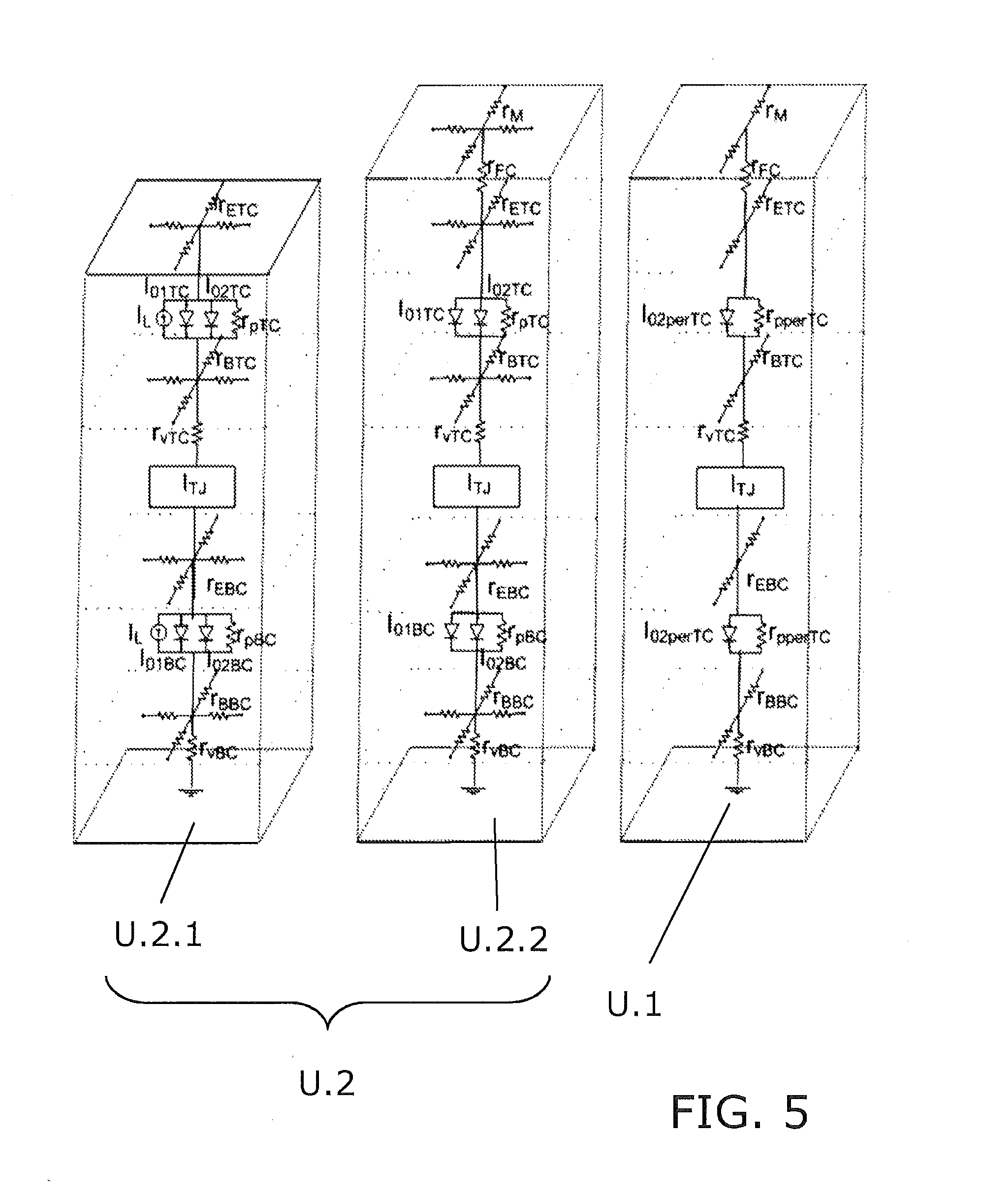
[0025]The present invention consists in a method implemented in a computer for the numerical simulation of a semiconductor device comprising one or more tunnel junctions, such as a multijunction solar cell.[0026]The semiconductor device has a main plane and is described by a model featuring circuit units distributed along this main plane that comprises interconnected elemental circuit units.[0027]The device is made up of a semiconductor structure which can be mainly depicted by layers where each layer has a specific function. The main plane is a reference plane so that the layers are essentially arranged in parallel to this main plane. This main plane is usually represented horizontally and the transversal direction which traverses the semiconductor structure is represented vertically.[0028]The method of the invention makes use of a model based on circuits of electronic components which allows working with said model instead of with the device by means of simulations that allows amo...
PUM
 Abstract
Description
Claims
Application Information