
Low Leakage Boundary Scan Device Design and Implementation

a scanning device and low leakage technology, applied in the direction of power consumption reduction, pulse technique, instruments, etc., can solve problems such as power drain, and achieve the effect of saving power

Active Publication Date: 2013-10-24
GLOBAL UNICHIP CORPORATION
View PDF7 Cites 0 Cited by
  • Summary
  • Abstract
  • Description
  • Claims
  • Application Information

AI Technical Summary

Benefits of technology

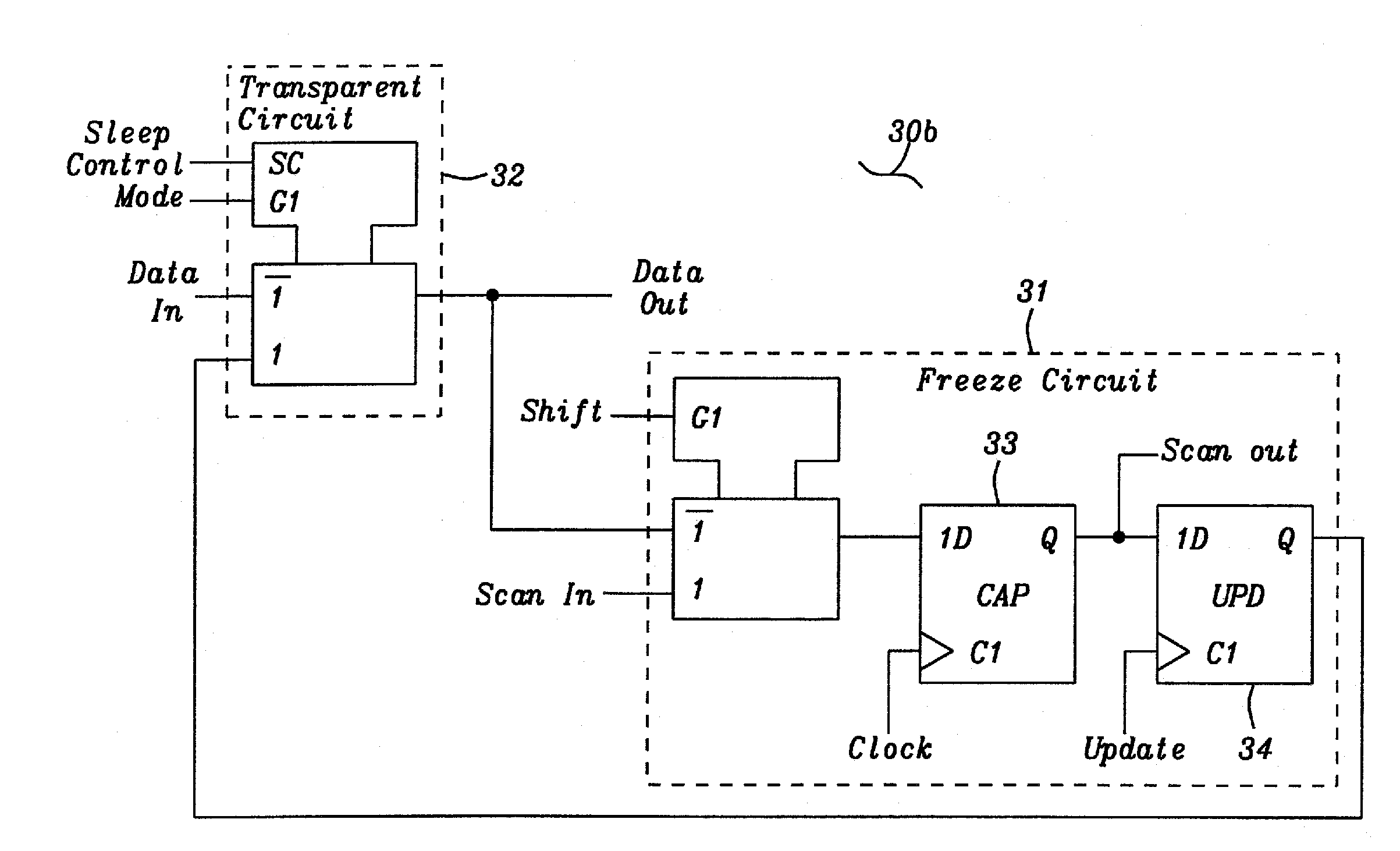
The present invention provides circuitry and control to block signals and isolate internal logic from unwanted signals in an integrated circuit device during sleep mode. This is accomplished by using a boundary-scan circuit with a freeze circuit and a transparent circuit. The transparent circuit is used to connect a pad device to internal logic and impose a sleep mode to prevent leakage currents. The invention also includes power-gating transistors to negate the effects of mode control and input transistors when a sleep mode is imposed. The transparent circuit can isolate logic blocks without affecting other components in the device. This allows for partial or total placement of logic blocks into sleep mode, resulting in improved power efficiency and reduced leakage currents during sleep mode.

Problems solved by technology

This leakage current is a source of power drain during sleep mode.

Method used


Image

  • Low Leakage Boundary Scan Device Design and Implementation
  • Low Leakage Boundary Scan Device Design and Implementation
  • Low Leakage Boundary Scan Device Design and Implementation

Examples


first embodiment

[0035]FIG. 4B is a circuit diagram 41 of first embodiment of the transparent circuit 32. When the sleep control is off, +V, the mode select signal G1 connects to two transistors, a p-channel device 42 and an n-channel device 43, which selects either input In0 (Data In) or input In1 (Scan In), to connect to the select circuits formed by the p-channel transistor 50 and the n-channel transistor 51, and the select circuit formed by the p-channel transistor 52 and the n-channel transistor 53. The output of the select circuits connect to the input of the output circuit formed by the p-channel transistor 54 and the n-channel transistor 55, where the output circuit provides an out put signal “Z”. Input I0 or I1 is selected by the application of the G1 signal from the p-channel transistor 42 to the gates of the selector circuit gates of the n-channel transistor 51 and the p-channel transistor 52 while the inverted G1 signal is applied to the selector circuit gates of the p-channel transistor...

second embodiment

[0039]When the sleep control is off, +V, in the circuit of the second embodiment, the mode select signal G1 connects to two transistors, a p-channel device 42 and an n-channel device 43, which selects either input In0 (Data In) or input In1 (Scan In). The mode select signal G1 controls the selection of the appropriate input to the select circuits formed by the p-channel transistor 50 and the n-channel transistor 51, and the select circuit formed by the p-channel transistor 52 and the n-channel transistor 53. The select circuits connect to the input of the output circuit formed by the p-channel transistor 54 and the n-channel transistor 55, where the output circuit provides an out put signal “Z”. Input I0 or I1 is selected by the application of the G1 signal from the p-channel transistor 42 to the gates of the n-channel transistor 51 and the p-channel transistor 52. At the same time an inverted G1 signal is applied to the selector circuit gates of the p-channel transistor 50 and the ...


PUM


Abstract

A boundary scan circuit containing a freeze circuit and a transparency circuit that provides a capability to selectively place portions of a system logic in a sleep mode and thereby conserving power. There are two transparency circuit configurations, one that connects to an input pad cell and one that connects to an output pad cell. The circuitry in the transparency circuit is controlled in such a manner as to establish at the output of transparency circuit a known logic state to control leakage current resulting from the circuitry of the various pad cell configurations, which further conserves power during sleep mode.

Description

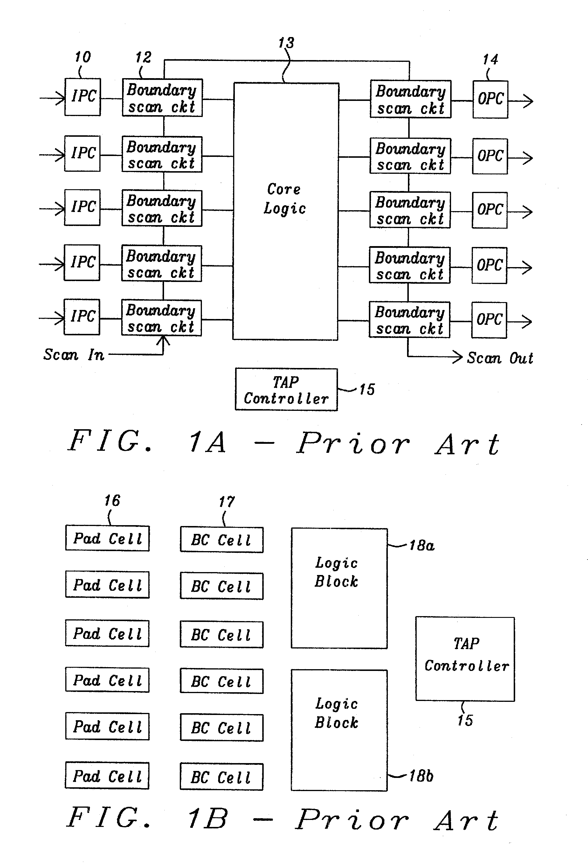
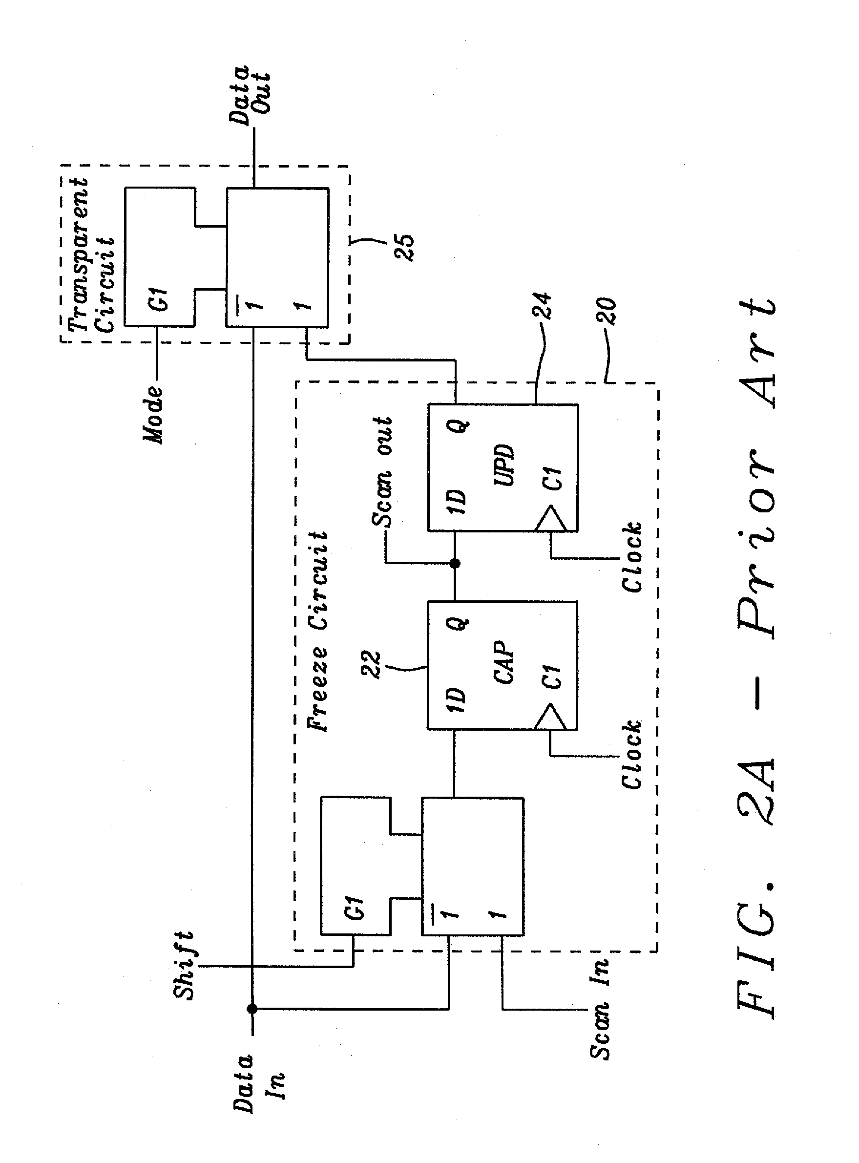
[0001]This is a Divisional application of U.S. patent application Ser. No. 12 / 802,678, filed on Jun. 10, 2010, and incorporated by reference in its entirety, and assigned to the same assigneeBACKGROUND OF THE INVENTION[0002]1. Field of Invention[0003]The present invention relates to boundary scan circuitry and in particular the creation and use of the boundary scan circuitry to reduce power consumption and leakage problems during sleep mode.[0004]2. Description of Related Art[0005]Boundary scan is an architecture defined by IEEE Std. 1149.1 that is used for testing circuitry 1) between packaged integrated circuit chips and 2) to force test signals upon the core logic within an integrated circuit chip, both without the need to physically probe connections on a physical package, or printed circuit board. Boundary scan has proven very useful in determining shorts and opens that may exist in the wiring between semiconductor chips mounted on a board or similar package. Because the bounda...

Claims


Application Information

Patent Timeline
Patent Type & Authority Applications(United States)
IPC IPC(8): H03K19/00
CPCH03K19/0008G01R31/318575H03K19/0016
Inventor TSAI, MIN-HSIU
Owner GLOBAL UNICHIP CORPORATION
Learn More