Electronic component

a technology of electronic components and components, applied in the direction of printed circuit parts, printed circuit non-printed electric components association, printed circuit final product manufacturing, etc., can solve the problems of vibration sound, reduce the frequency of vibration sound, reduce the size, and facilitate the mounting of chip components on the circuit board

Active Publication Date: 2013-10-31
MURATA MFG CO LTD
View PDF3 Cites 58 Cited by
  • Summary
  • Abstract
  • Description
  • Claims
  • Application Information

AI Technical Summary

Benefits of technology

[0046]The mounting of the chip component, such as the multilayer ceramic capacitor, on the circuit board by using the electronic component indicated in various preferred embodiments of the present invention allows the occurrence of the vibration sound to be significantly reduced or prevented. In addition, the structure is simple to enable a reduction in size and it is easy to mount the chip component on the circuit board. Furthermore, it is possible to ensure mounting strength and electrical characteristics similar to those of common mounting structures in the related art.

Problems solved by technology

If the solder spreads to central portions of the end surfaces of the chip component via the insulating substrate, both ends of the chip component is strongly restrained by the solder to cause vibration of the chip component to be easily transmitted to the circuit board via the insulating substrate to possibly cause a vibration sound.

Method used


Image

  • Electronic component
  • Electronic component
  • Electronic component

Examples


Embodiment Construction

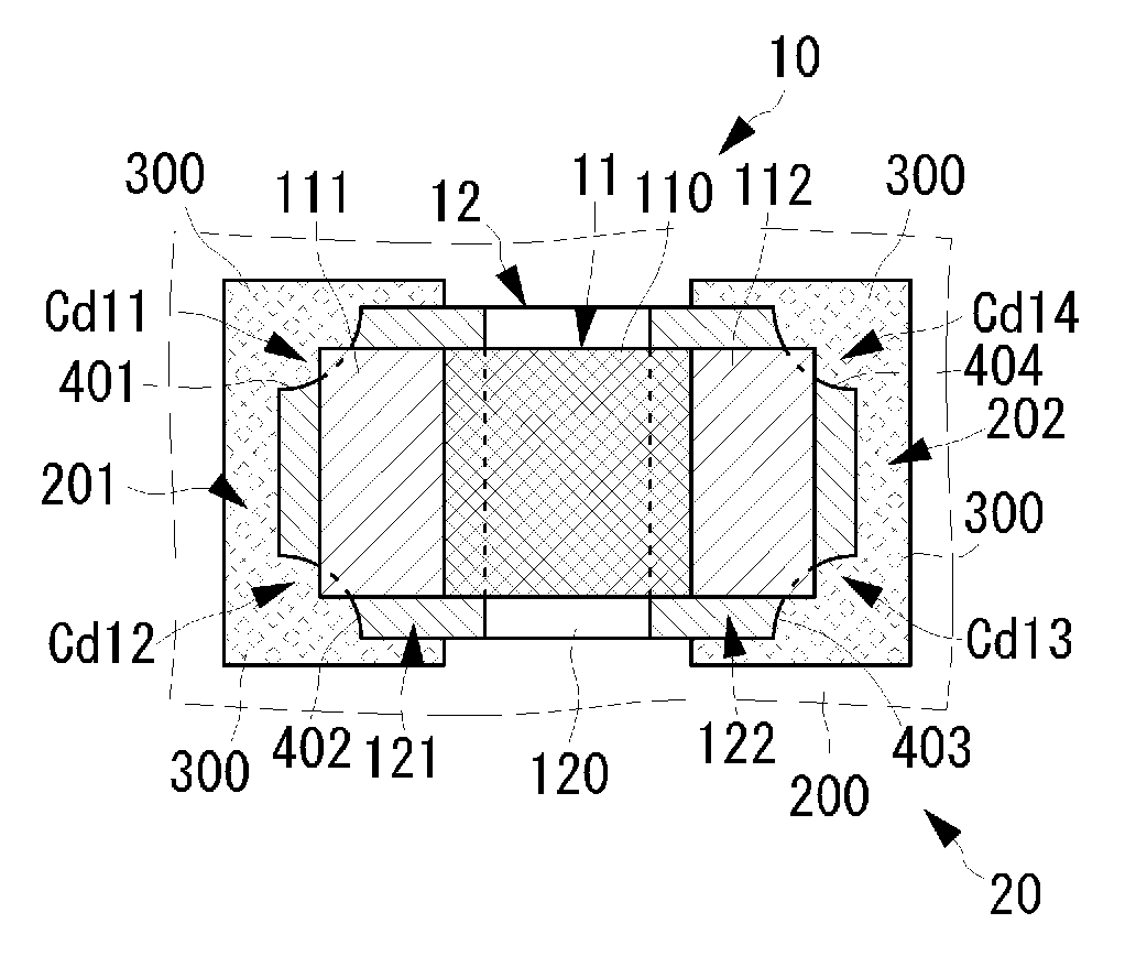
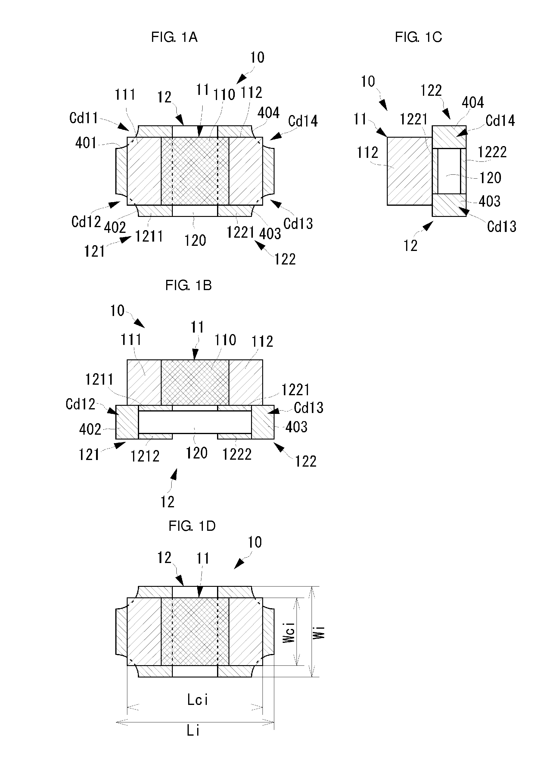
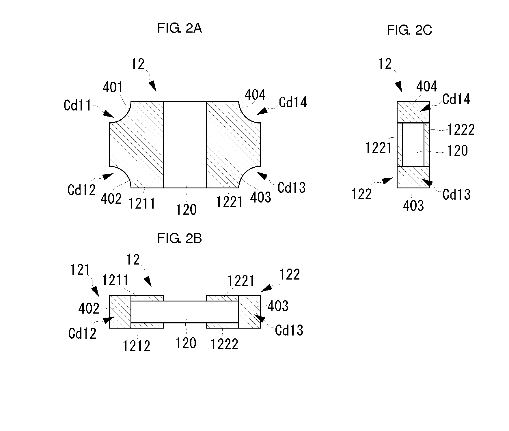
[0064]An electronic component including an interposer according to a first preferred embodiment of the present invention will herein be described with reference to the attached drawings. FIGS. 1A-1D include orthographic views illustrating an exemplary structure of an electronic component 10 including an interposer 12 according to the present preferred embodiment and a diagram indicating the relationship between the shape of the interposer 12 and that of a multilayer ceramic capacitor 11. FIGS. 2A-2C are orthographic views of the interposer 12 according to the present preferred embodiment. FIGS. 3A-3C are orthographic views indicating a state in which the electronic component 10 according to the present preferred embodiment is mounted on a circuit board 20. In the orthographic views illustrated in FIGS. 1A-1C, FIGS. 2A-2C, and FIGS. 3A-3C, FIG. 1A, FIG. 2A, and FIG. 3A are plan views; FIG. 1B, FIG. 2B, and FIG. 3B are side views in the length direction; and FIG. 1C, FIG. 2C and FIG. ...


PUM

PropertyMeasurementUnit
widthaaaaaaaaaa
widthaaaaaaaaaa
widthaaaaaaaaaa

Abstract

In an electronic component, upper surface electrodes are located on one main surface of an insulating substrate of an interposer on which a multilayer ceramic capacitor is mounted. The insulating substrate has substantially the same shape as that of the multilayer ceramic capacitor, viewed from a direction perpendicular or substantially perpendicular to the main surface, and has the multilayer ceramic capacitor mounted thereon so that the length direction of the multilayer ceramic capacitor substantially coincides with the length direction of the insulating substrate. The insulating substrate includes cutouts that include connection electrodes, respectively, and that are located at the four corners viewed from the direction perpendicular or substantially perpendicular to the main surface. The upper surface electrodes on the one main surface are connected via the connection electrodes to lower surface electrodes, respectively, that are located on the other main surface and are connected to a circuit board.

Description

BACKGROUND OF THE INVENTION[0001]1. Field of the Invention[0002]The present invention relates to an electronic component that is used to mount a chip component, such as a multilayer ceramic capacitor, on a circuit board and that includes an interposer.[0003]2. Description of the Related Art[0004]Many chip components, particularly, many compact multilayer ceramic capacitors are currently used in mobile terminals including cellular phones. The multilayer ceramic capacitors are each composed of a rectangular component body that functions as a capacitor and outer electrodes formed at both opposing ends of the component body.[0005]In general, as indicated in Japanese Unexamined Patent Application Publication No. 8-55752, the multilayer ceramic capacitor has heretofore been electrically and physically connected to a circuit board of a mobile terminal by directly placing and holding the outer electrodes on a mounting land on the circuit board and joining the mounting land to the outer elec...

Claims


Application Information

Patent Timeline
Patent Type & Authority Applications(United States)
IPC IPC(8): H05K1/18
CPCH05K1/18H05K1/181H05K3/3442H05K2201/09145H05K2201/10015H05K2201/10378H05K2201/2045Y02P70/50H01G2/02H01G2/06
Inventor HATTORI, KAZUOYAMADA, TADATERUFUJIMOTO, ISAMU
Owner MURATA MFG CO LTD
Why Eureka
Try Eureka