Multi-Gate Devices with Replaced-Channels and Methods for Forming the Same

a technology of multi-gate devices and channels, applied in the direction of basic electric elements, semiconductor devices, electrical apparatus, etc., can solve the problems of epitaxy source and drain region impurities being adversely diffused into the channel, and the need for higher drive current of the transistors

Active Publication Date: 2013-10-31
TAIWAN SEMICON MFG CO LTD
View PDF26 Cites 83 Cited by
  • Summary
  • Abstract
  • Description
  • Claims
  • Application Information

AI Technical Summary

Problems solved by technology

With the increasing down-scaling of integrated circuits and increasingly demanding requirements to the speed of integrated circuits, transistors need to have higher drive currents with smaller dimensions.
Furthermore, the impurities in the epitaxy source and drain regions may be adversely diffused into the channel in the subsequent thermal processes.

Method used


Image

  • Multi-Gate Devices with Replaced-Channels and Methods for Forming the Same
  • Multi-Gate Devices with Replaced-Channels and Methods for Forming the Same
  • Multi-Gate Devices with Replaced-Channels and Methods for Forming the Same

Examples


Embodiment Construction

[0006]The making and using of the embodiments of the disclosure are discussed in detail below. It should be appreciated, however, that the embodiments provide many applicable inventive concepts that can be embodied in a wide variety of specific contexts. The specific embodiments discussed are illustrative, and do not limit the scope of the disclosure.

[0007]Fin Field-Effect Transistors (FinFETs) and the methods of forming the same are provided in accordance with various embodiments. The intermediate stages of forming the FinFETs are illustrated. The variations of the embodiments are discussed. Throughout the various views and illustrative embodiments, like reference numbers are used to designate like elements.

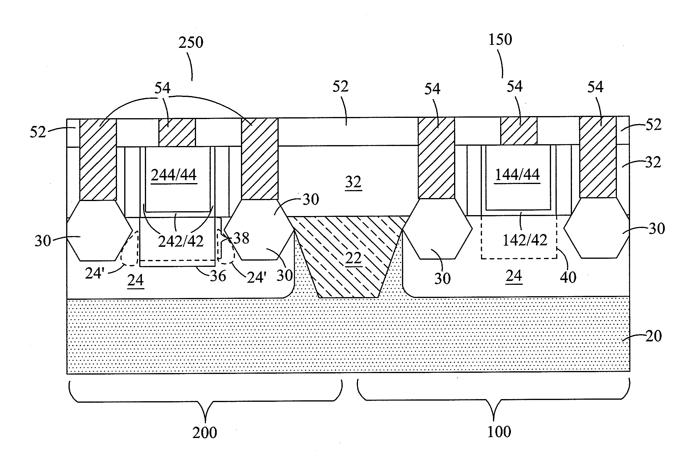
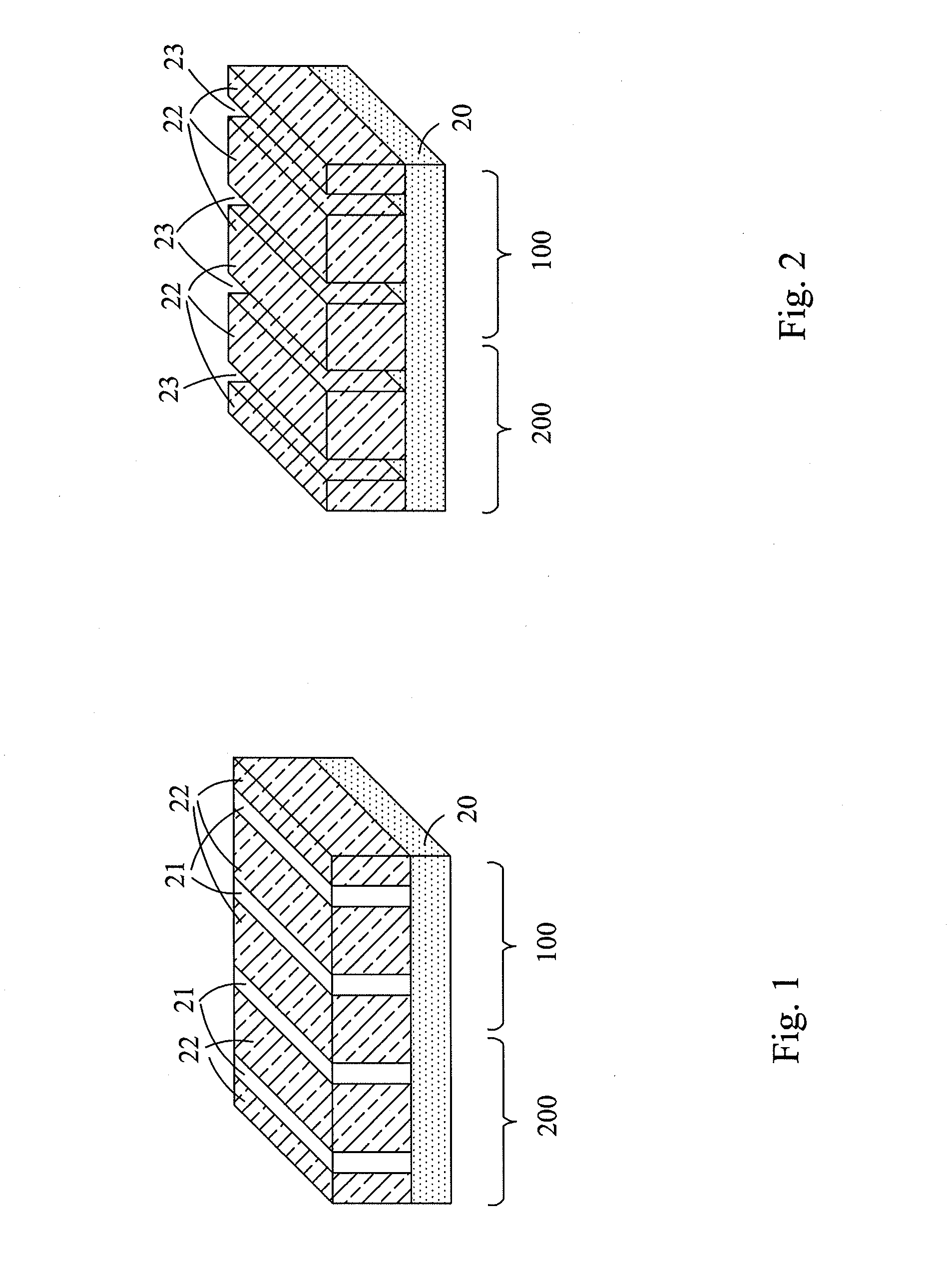
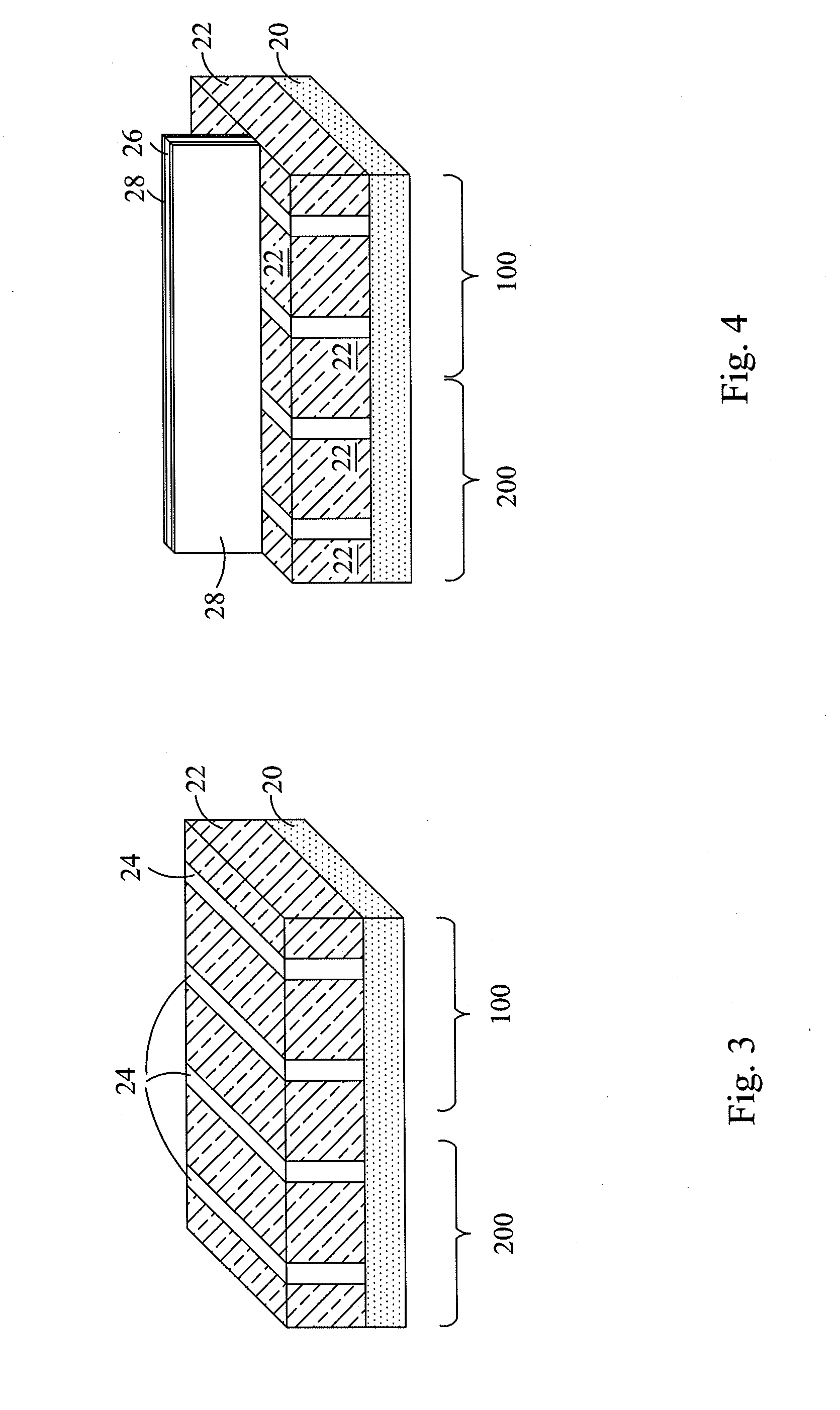
[0008]FIGS. 1 through 13 are cross-sectional views and perspective views of intermediate stages in the manufacturing of Fin Field-Effect Transistors (FinFETs) in accordance with some exemplary embodiments. FIG. 1 illustrates a perspective view of an initial structure. The initia...


PUM


Abstract

A device includes a semiconductor substrate, isolation regions in the semiconductor substrate, and a Fin Field-Effect Transistor (FinFET). The FinFET includes a channel region over the semiconductor substrate, a gate dielectric on a top surface and sidewalls of the channel region, a gate electrode over the gate dielectric, a source/drain region, and an additional semiconductor region between the source/drain region and the channel region. The channel region and the additional semiconductor region are formed of different semiconductor materials, and are at substantially level with each other.

Description

CROSS-REFERENCE TO RELATED APPLICATION[0001]This application relates to the following commonly-assigned co-pending U.S. patent application: application Ser. No. 13 / 356,769, filed Jan. 24, 2012, and entitled “FinFETs and Methods for Forming the Same;” which application is hereby incorporated herein by reference.BACKGROUND[0002]With the increasing down-scaling of integrated circuits and increasingly demanding requirements to the speed of integrated circuits, transistors need to have higher drive currents with smaller dimensions. Fin Field-Effect Transistors (FinFETs) were thus developed. FinFETs have increased channel widths. The increase in the channel widths is achieved by forming channels that include portions on the sidewalls of semiconductor fins and portions on the top surfaces of the semiconductor fins. Since the drive currents of transistors are proportional to the channel widths, the drive currents of the FinFETs are increased.[0003]In an existing FinFET formation process, Sh...

Claims


Application Information

Patent Timeline
Patent Type & Authority Applications(United States)
IPC IPC(8): H01L29/78H01L21/336
CPCH01L29/1054H01L29/66545H01L29/66795H01L29/785H01L29/0653H01L21/30604H01L21/31055H01L21/823431H01L21/823437H01L21/823481H01L21/823821H01L27/0924H01L29/165H01L29/6656H01L29/7848H01L29/7849
Inventor KUO, CHIH-WEICHAO, YUAN-SHUNCHEN, HOU-YUYANG, SHYH-HORNG
Owner TAIWAN SEMICON MFG CO LTD
Why Eureka
Try Eureka