

Field effect transistors with reduced parasitic resistances and method
a field effect transistor and parasitic resistance technology, applied in transistors, semiconductor devices, electrical equipment, etc., can solve the problems of only partially contacted source/drain regions, uncontacted source/drain regions, negative impact on device performance, etc., to reduce s/d dopant deactivation, reduce s/d strain reduction, and reduce s/d dopant diffusion
- Summary
- Abstract
- Description
- Claims
- Application Information
AI Technical Summary
Benefits of technology
Problems solved by technology
Method used
Image

Examples
Embodiment Construction
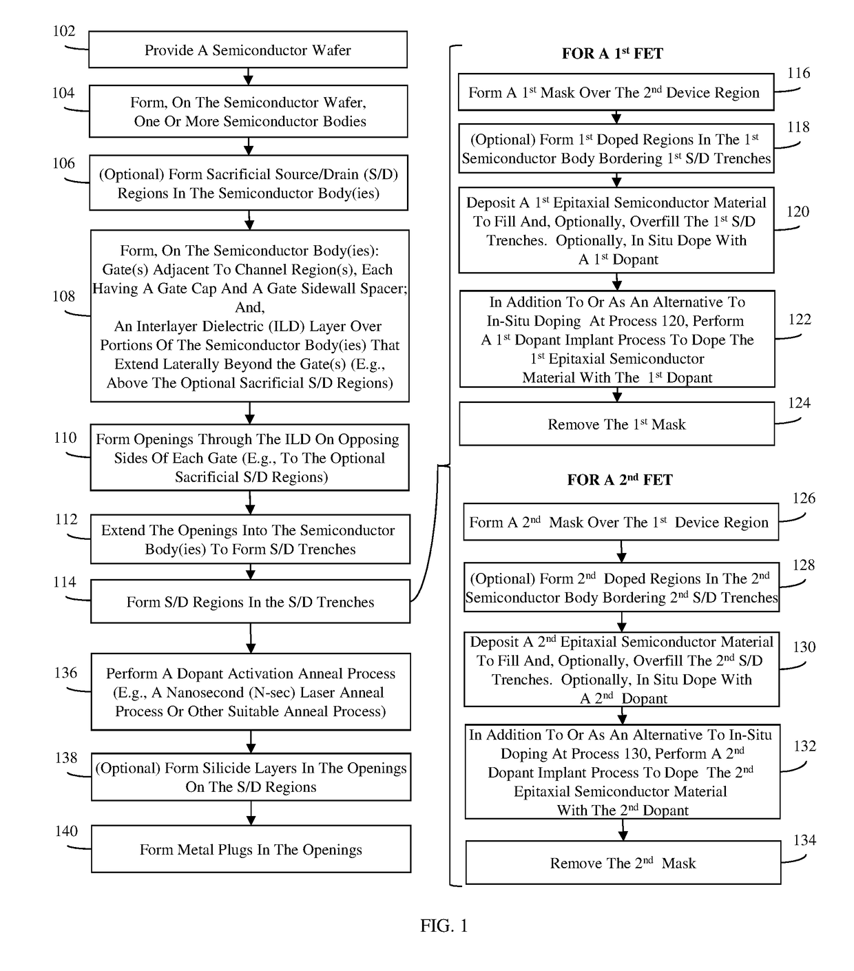
[0018]As mentioned above, as complementary metal oxide semiconductor (CMOS) technologies scale to smaller nodes, smaller critical dimensions can lead to problems that negatively impact device performance. For example, with field effect transistors (FETs), smaller critical dimensions can lead to an increase in parasitics and, particularly, an increase in parasitic resistances, such as metal plug resistance and source / drain region resistance. Additionally, smaller critical dimensions can lead to overlay errors when lithographically patterning openings for metal plugs that will contact source / drain regions. As a result of these overlay errors, the source / drain regions may be uncontacted or only partially contacted.
[0019]Additionally, in conventional field effect transistor (FET) processing, some processes (e.g., processes performed during replacement metal gate formation), which are performed after source / drain dopant activation and before middle of the line (MOL) processing, are assoc...
PUM
 Abstract
Description
Claims
Application Information