Current Limit Circuit Architecture For Low Drop-Out Voltage Regulators

a voltage regulator and current limit circuit technology, applied in the direction of electric variable regulation, emergency protective arrangements for limiting excess voltage/current, instruments, etc., can solve the problem of unfavorable overall circuit stability, and cannot guarantee the correct current limit behavior for the entire range of possible output voltages

Inactive Publication Date: 2013-11-07
TOWER SEMICONDUCTOR
View PDF3 Cites 52 Cited by
  • Summary
  • Abstract
  • Description
  • Claims
  • Application Information

AI Technical Summary

Benefits of technology

[0007]Accordingly, the present invention provides a current limiting circuit that provides protection for high power applications designed to protect an associated regulator and load from external shorts and excessive current consumption by the load circuitry. The current limiting circuit of the present invention limits the load current, when the load current exceeds a predetermined threshold current, by lowering the output voltage, thereby protecting output stage devices from undesirably high currents.

Problems solved by technology

Using current sampling circuitry to measure current through the output pass circuit of the voltage regulator undesirably complicates the process of achieving overall circuit stability.
Moreover, the current limiting technique is limited by the headroom required to operate the current sampling circuitry, and therefore does not guarantee correct current limiting behavior for the entire range of possible output voltages, particularly output voltages close to 0 Volts.

Method used


Image

  • Current Limit Circuit Architecture For Low Drop-Out Voltage Regulators
  • Current Limit Circuit Architecture For Low Drop-Out Voltage Regulators
  • Current Limit Circuit Architecture For Low Drop-Out Voltage Regulators

Examples


Embodiment Construction

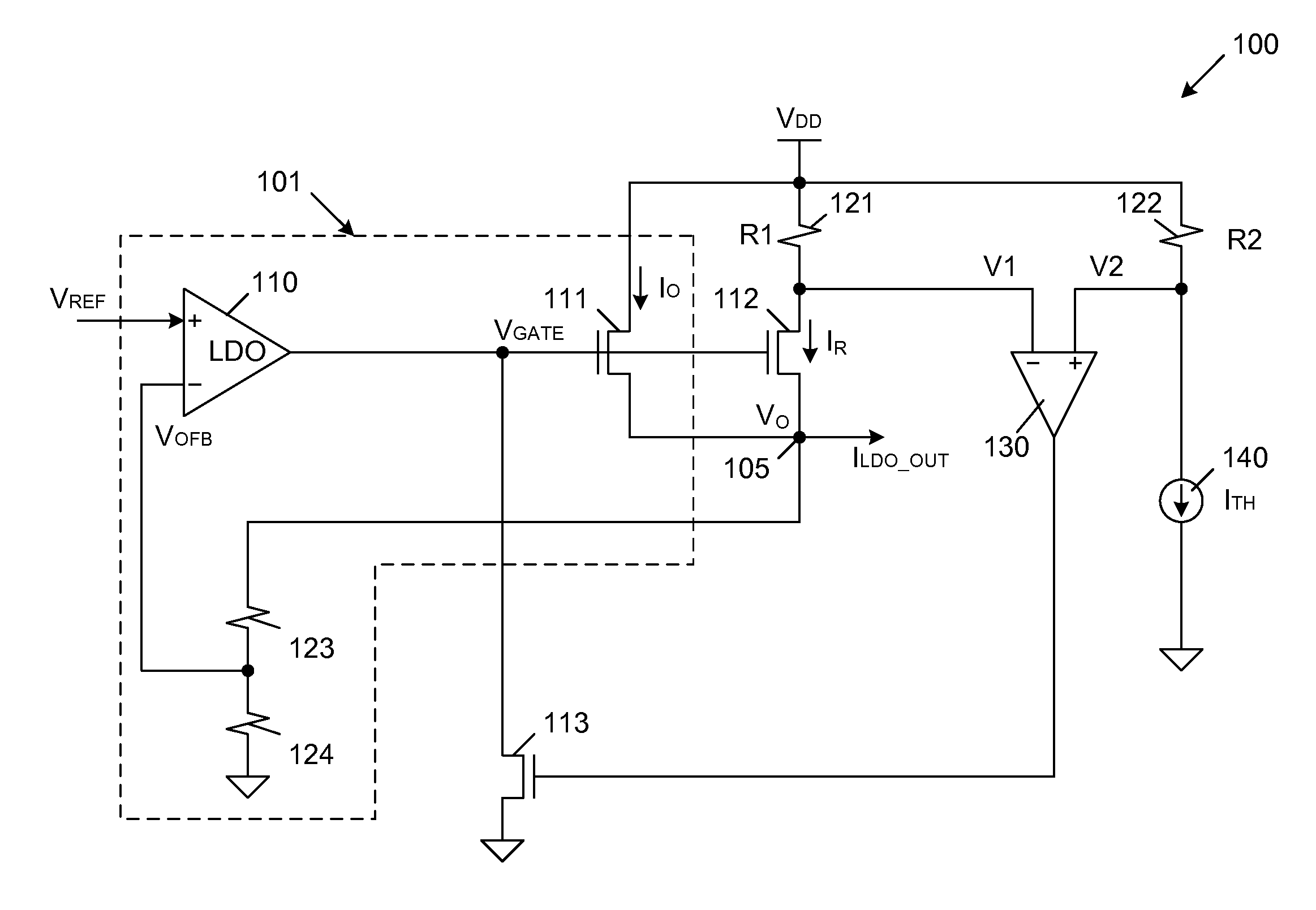
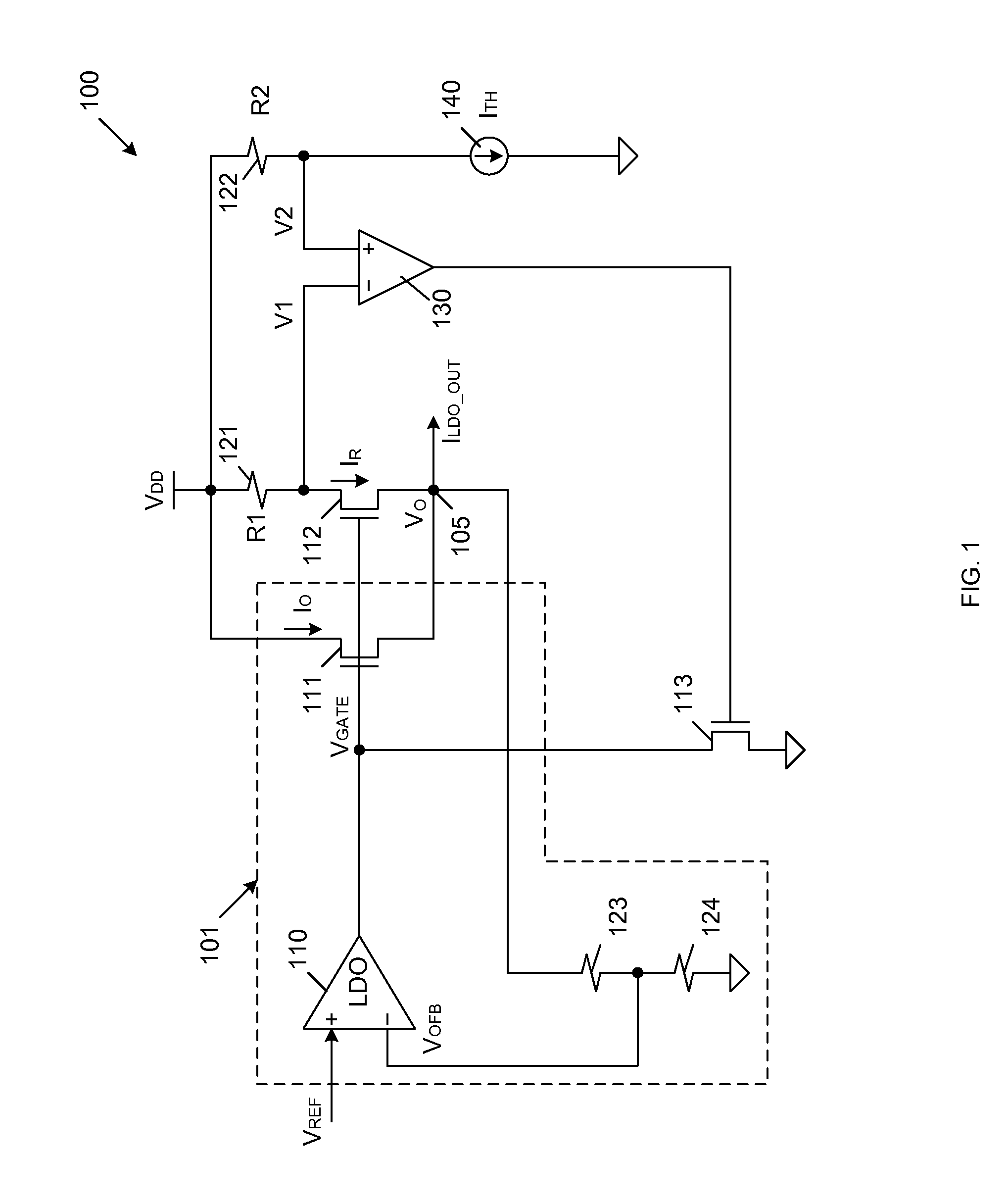
[0014]FIG. 1 is a circuit diagram of a current limiting circuit 100 for use with a low dropout (LDO) voltage regulator 101. Voltage regulator 101 includes linear amplifier 110, output stage transistor 111 and resistors 123-124 in accordance for one embodiment of the present invention. Current limiting circuit 100 includes n-channel MOS transistors 112-113, resistors 121-122, amplifier 130 and constant current source 140. As described in more detail below, current limiting circuit 100 provides an output voltage VO on output terminal 105.

[0015]Linear amplifier 110 includes a non-inverting input coupled to receive a reference voltage VREF, and an inverting input coupled to receive an output feedback voltage VOFB. In accordance with one embodiment, the output feedback voltage VOFB is derived from a resistive divider circuit that includes resistors 123-124, which are connected between the output terminal 105 and the ground supply terminal as illustrated. In the illustrated embodiment, re...


PUM


Abstract

A current limiting circuit for a linear regulator includes an output stage transistor and a replica transistor, which have gates coupled to receive an output voltage from a linear amplifier and sources coupled to load circuitry. A drain of the output stage transistor is coupled to a VDD supply terminal, while a drain of the replica transistor is coupled to the VDD supply terminal through a first resistor. The output stage transistor and replica transistor are operated in saturation, such that proportional currents flow through these transistors. The voltage drop across the first resistor provides a first voltage, which is applied to a second amplifier. A reference voltage is also applied to the second amplifier. When the first voltage becomes less than the reference voltage, a feedback transistor is enabled to pull down the output voltage of the linear amplifier, thereby limiting the output current supplied to the load circuitry.

Description

FIELD OF THE INVENTION[0001]The present invention relates to a current limiting circuit for use in connection with low drop out voltage regulators.RELATED ART[0002]U.S. Pat. No. 7,986,499 to Wang et al. describes a conventional current limiting circuit for limiting a current passing through an output pass circuit of a voltage regulator. The current limiting circuit includes a current sampling circuit for sampling the current passing through the output pass circuit to obtain a duplicated current that is proportional to the current passing through the output pass circuit. As used herein, a current sampling circuit is a circuit that copies the gate, source and drain voltages of an output stage transistor (e.g., MPass of FIG. 4) to a scaled transistor (e.g., MP1 of FIG. 4). Note that the source voltages of transistors MPass and MP1 are equalized through the transistors MP3, MP2, MN1 and MN2 of Wang et al.[0003]The current limiting circuit of Wang et al. also includes a current mirror ci...

Claims


Application Information

Patent Timeline
Patent Type & Authority Applications(United States)
IPC IPC(8): H02H9/02
CPCG05F1/573
Inventor LERNER, VALENTINPOLLAK, DAN
Owner TOWER SEMICONDUCTOR
Why Eureka
Try Eureka