Organic Light Emitting Device and Method of Fabricating the Same

a light-emitting device and organic technology, applied in the direction of organic semiconductor devices, thermoelectric devices, solid-state devices, etc., can solve the problems of increasing driving voltage and reducing lifespan and efficiency of devices, and achieve the effect of improving efficiency and lifespan

Active Publication Date: 2013-11-28
LG DISPLAY CO LTD
View PDF13 Cites 30 Cited by
  • Summary
  • Abstract
  • Description
  • Claims
  • Application Information

AI Technical Summary

Benefits of technology

[0009]An object of the present invention is to provide an organic light emitting device capable of improving efficiency and lifespan by removing an interfacial barrier between hole transport layers and a method of fabricating the same.

Problems solved by technology

Hereupon, organic light emitting devices that display an image by adjusting an amount of light emitted from an organic light emitting layer are recently receiving attention as flat panel display devices having reduced weight and volume, which are drawbacks of cathode ray tubes (CRTs).
Accordingly, driving voltage may increase and lifespan and efficiency of the device may decrease.

Method used


Image

  • Organic Light Emitting Device and Method of Fabricating the Same
  • Organic Light Emitting Device and Method of Fabricating the Same
  • Organic Light Emitting Device and Method of Fabricating the Same

Examples


first embodiment

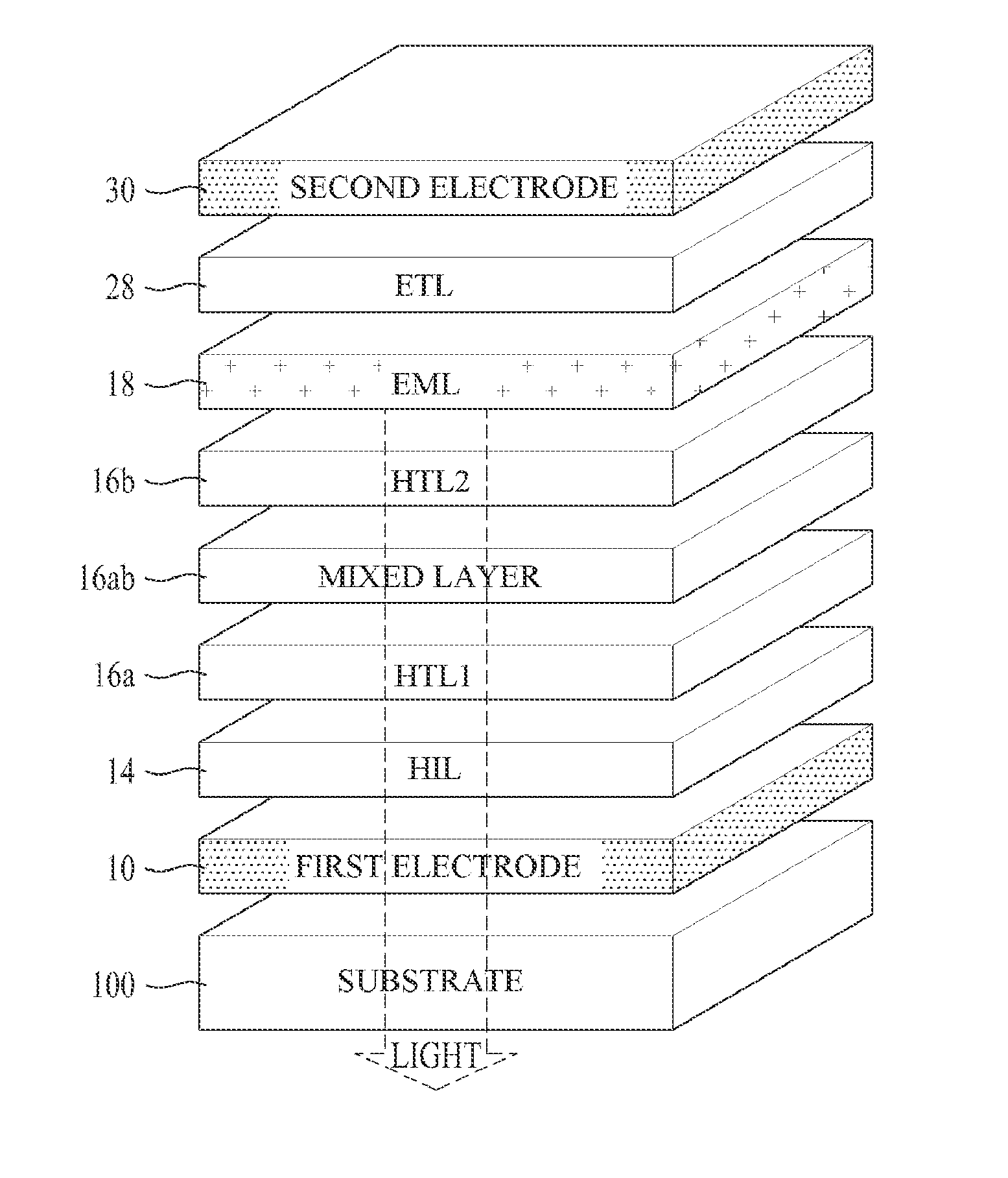
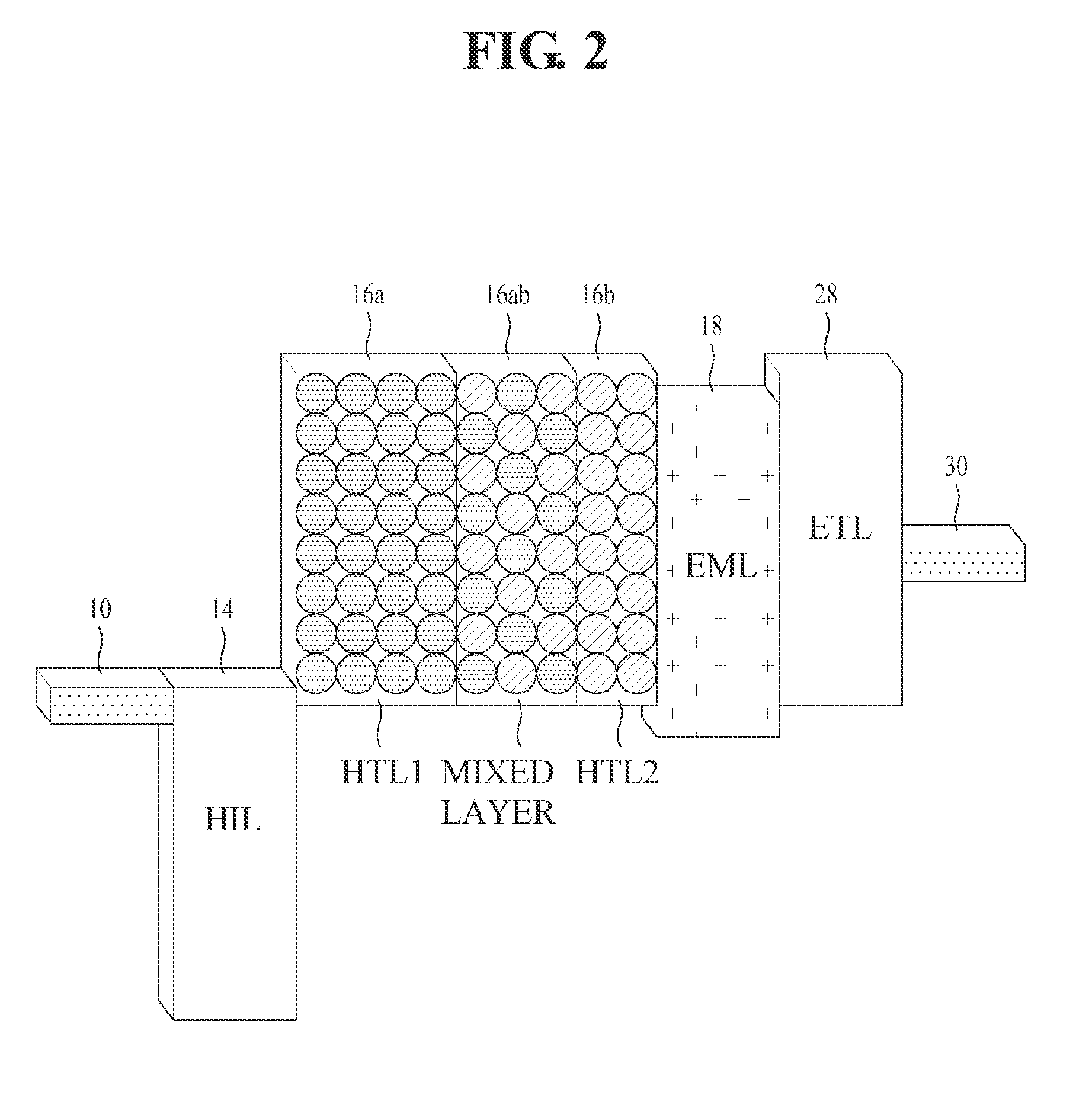
[0025]FIG. 1 is a perspective view illustrating an organic light emitting device according to a FIG. 2 is an energy band diagram of the organic light emitting device of FIG. 1

[0026]With reference to FIGS. 1 and 2, an organic light emitting device according to the first embodiment includes a first electrode 10, organic layers including a light emitting layer 18, and a second electrode 30. When the organic light emitting device applies a voltage to a first electrode 10 and a second electrode 30, holes injected from the first electrode 10 and electrons injected from the second electrode are recombined to create excitons that emit light when falling from an excited state to a ground state.

[0027]The first electrode 10 as an anode may be formed of a transparent conductive material, for example, a transparent conductive oxide (TCO) such as indium tin oxide (ITO) and indium zinc oxide (IZO).

[0028]The second electrode 30 as a cathode may be formed of a reflective metallic material such as a...

second embodiment

[0033]FIG. 3 is a perspective view illustrating an organic light emitting device according to a FIG. 4 is an energy band diagram of the organic light emitting device of FIG. 3.

[0034]With reference to FIGS. 3 and 4, an organic light emitting device according to the second embodiment includes a first electrode 110 and a second electrode 130, which are formed on a substrate opposite to each other, and a first stack 210, a charge generation layer 122, and a second stack 220, which are laminated between the first electrode 110 and the second electrode 150. Such an organic light emitting device having a multi-stack structure includes stacks respectively including light emitting layers that emit light with different colors. White light is embodied when light beams having different colors emitted from the light emitting layers of the stacks are mixed. The organic light emitting device according to the second embodiment realizes white light by mixing blue light emitted from the first light ...


PUM


Abstract

An organic light emitting device includes a substrate, a first electrode on the substrate, a second electrode, a first stack on the first electrode and including a hole injection layer, a first hole transport layer, a first mixed layer, a second hole transport layer, a first light emitting layer, and a first electron transport layer sequentially laminated, a second stack between the first stack and the second electrode and including a third hole transport layer, a fourth hole transport layer, a second light emitting layer, and a second electron transport layer sequentially laminated, and a charge generation layer between the first stack and the second stack to control charge balance between the first and second stacks. The first mixed layer includes materials used to form the first and second hole transport layers.

Description

[0001]This application claims the benefit of priority of Korean Patent Application No. 10-2012-0054490, filed on May 2012, which is hereby incorporated by reference as if fully set forth herein.BACKGROUND[0002]1. Field of the Disclosure[0003]The present disclosure relates to an organic light emitting device and, more particularly, to an organic light emitting device with improved efficiency and lifespan.[0004]2. Discussion of the Related Art[0005]For an image display device that displays a variety of information on a screen as a core technology in advanced information and communication, there is continuous progress in development of slim, lightweight, and portable devices with improved performance. Hereupon, organic light emitting devices that display an image by adjusting an amount of light emitted from an organic light emitting layer are recently receiving attention as flat panel display devices having reduced weight and volume, which are drawbacks of cathode ray tubes (CRTs).[000...

Claims


Application Information

Patent Timeline
Patent Type & Authority Applications(United States)
IPC IPC(8): H01L51/50H01L51/56
CPCH01L51/5064H01L51/56H01L2251/558H01L27/3209H01L51/5008H10K59/32H10K30/865H10K50/156H10K2102/351H10K85/111H10K50/16H10K50/15H10K71/00
Inventor HEO, JEONG-HAENGLEE, JAE-MANSHIN, JEONG-KYUNCHO, GWI-JEONGAHN, SO-YEON
Owner LG DISPLAY CO LTD
Why Eureka
Try Eureka