Capacitive fingerprint sensor

Active Publication Date: 2013-11-28
SILICON DISPLAY TECH CO LTD
View PDF2 Cites 32 Cited by
  • Summary
  • Abstract
  • Description
  • Claims
  • Application Information

AI Technical Summary

Benefits of technology

The present invention provides a fingerprint sensor that can enhance sensing sensitivity by primarily sensing and amplifying a difference between capacitances and secondarily amplifying an amplified signal within a pixel again. This allows for sufficient currents to be generated and improves sensing sensitivity. Additionally, a protective film can be formed on the sensor to improve resistance to ESD damage or physical impact.

Problems solved by technology

However, in the conventional capacitive fingerprint sensor, when the fingerprint capacitance Cfp is small, namely, a difference between the capacitances based on ridges of the fingerprint is small, ΔVg-T2 (a difference between the voltages applied to the gate of the T2) becomes smaller, thereby reducing fingerprint sensing sensitivity.
and the conventional capacitive fingerprint sensor has a limit to increase a difference between the Isignal and the Idark, thereby generating a limit to enhance the sensing sensitivity.
Thus, in the way of the conventional capacitive fingerprint sensor which senses the fingerprint formed by using the fingers and a protective film of an upper part of the sensor as a dielectric, since the protective film of the upper part of the sensor may not be formed to be thick, the conventional capacitive fingerprint sensor is certainly weak to ESD damage or physical damage.

Method used


Image

  • Capacitive fingerprint sensor
  • Capacitive fingerprint sensor
  • Capacitive fingerprint sensor

Examples


Embodiment Construction

[0048]Exemplary embodiments according to the present invention will now be described more fully hereinafter with reference to the accompanying drawings so that those having ordinary skill in the art can easily embody. This invention may, however, be embodied in different forms and should not be construed as limited to the exemplary embodiments set forth herein. To clearly explain the present invention, in the drawings, the parts which have no relation with the explanation are omitted. Like numbers refer to like elements throughout the specification.

[0049]Hereinafter, the detailed technical contents to be carried out by the present invention will be described in detail with reference to the accompanying drawings.

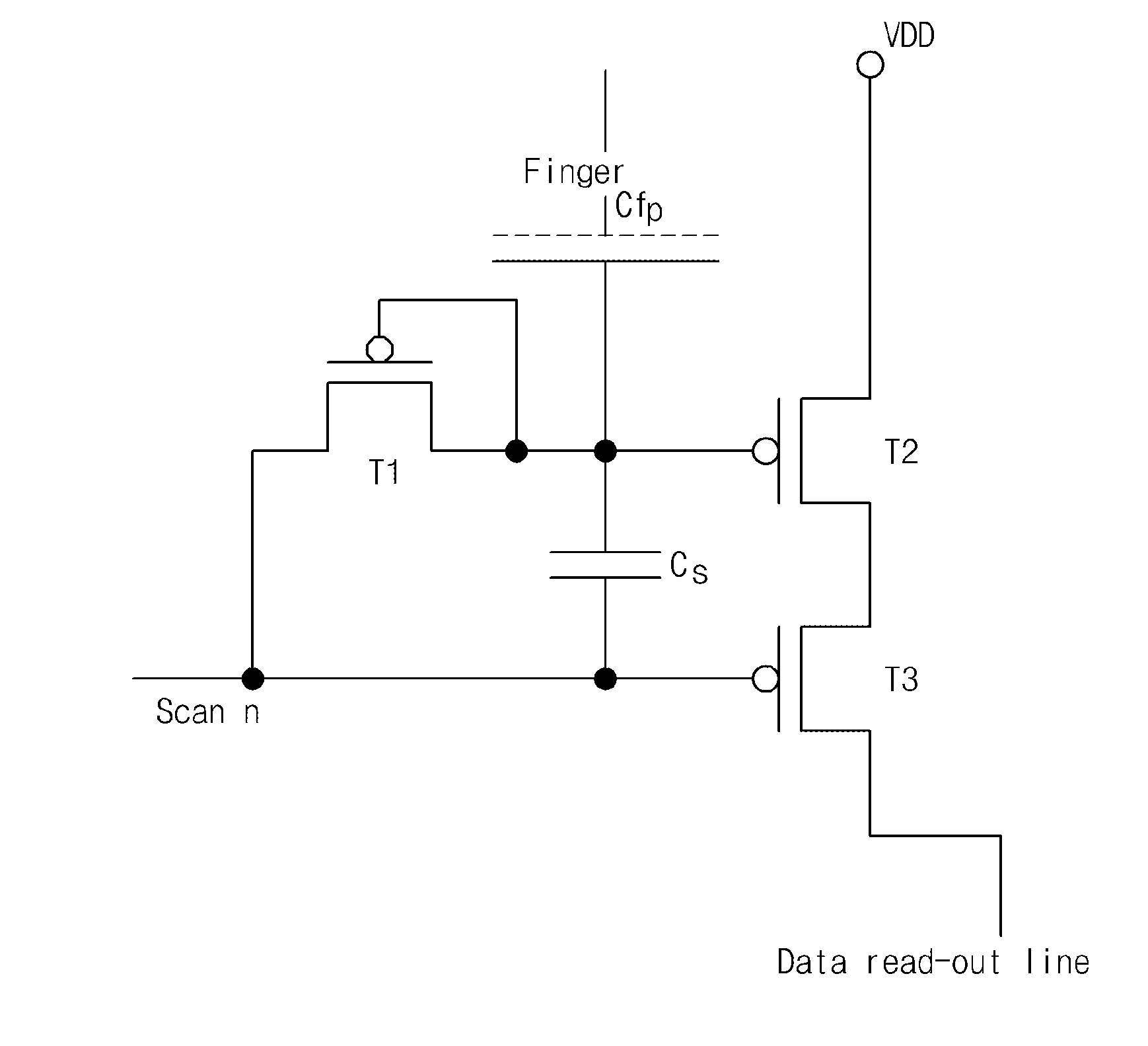
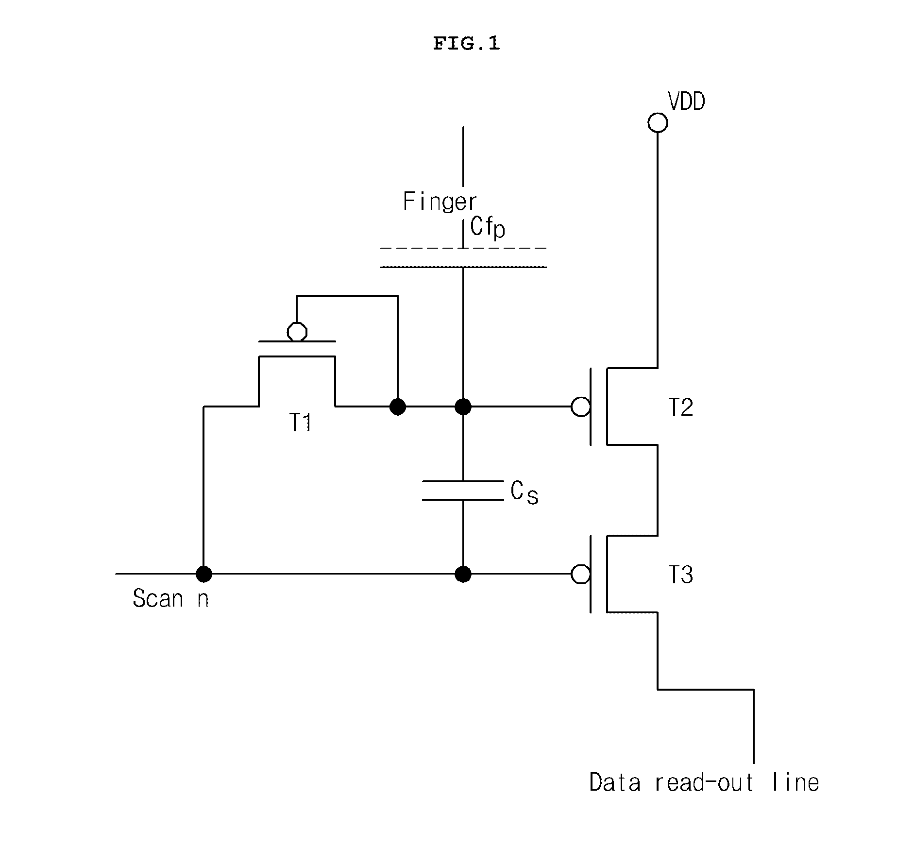
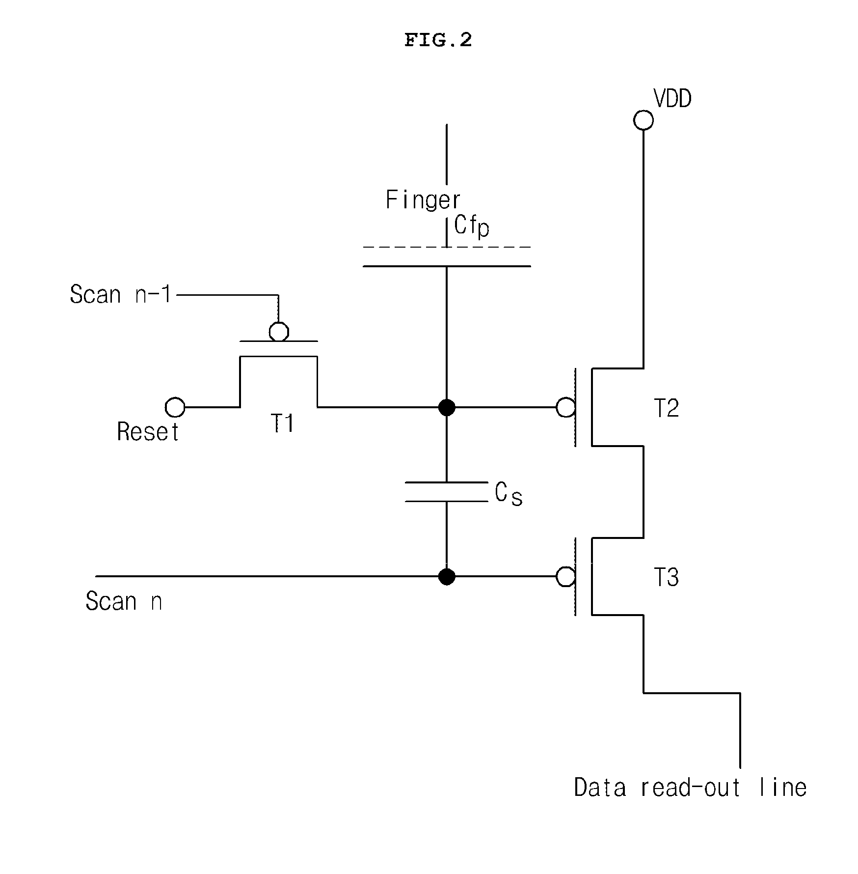
[0050]A capacitive fingerprint sensor according to exemplary embodiments of the present invention is characterized in that due to a difference between gate voltages of a first transistor T1 caused by a difference between fingerprint capacitances, the amount of currents flowin...


PUM


Abstract

The capacitive fingerprint sensor according to the exemplary embodiments of the present invention includes: a fingerprint sensing electrode Cfp for sensing a human fingerprint; a first transistor T1 in which the amount of currents flowing therethrough changes depending on an output voltage of the fingerprint sensing electrode Cfp; a second transistor T2 in which the amount of currents flowing therethrough changes due to a difference between the currents flowing through the first transistor T1; and a third transistor T3 which resets a gate electrode of the first transistor T1 and provides capacitive coupling with the gate electrode of the first transistor T1 via a pulse signal.

Description

CROSS REFERENCE TO RELATED APPLICATIONS[0001]This application is a Continuation of PCT International Application No. PCT / KR2012 / 004031 filed on May 22, 2012. The entire contents of all of the above application are hereby incorporated by reference into the present application.BACKGROUND OF THE INVENTION[0002]1. Field of the Invention[0003]The present invention relates to a capacitive fingerprint sensor, more specifically, a capacitive fingerprint sensor which is able to enhance sensing sensitivity and is resistant to ESD damage or a physical impact.[0004]2. Description of the Related Arts[0005]FIG. 1 through FIG. 4 are equivalent circuit views illustrating a capacitive type fingerprint sensor using a thin film transistor according to some exemplary embodiments of a conventional art.[0006]As illustrated in FIG. 1, the conventional capacitive type fingerprint sensor using the thin film transistor uses an active pixel structure to thereby include a source follower such as a T2 within a ...

Claims


Application Information

Patent Timeline
IPC IPC(8): H03K17/975
CPCH03K17/9622G06V40/1306
Inventor KANG, MOON HYOHUR, JI HO
Owner SILICON DISPLAY TECH CO LTD
Why Eureka
Try Eureka