Method of manufacturing a three dimensional photonic device by two photon absorption polymerization

a three-dimensional photonic device and photon absorption polymerization technology, applied in the direction of optical waveguide light guide, instruments, applications, etc., can solve the problems of high positioning accuracy, difficult integration of optical waveguides in a single device, and integration of optical waveguides with free-space micro-optical components and micromechanical structures, so as to improve the relative alignment

Inactive Publication Date: 2013-11-28
GLOBALFOUNDRIES INC
View PDF2 Cites 28 Cited by
  • Summary
  • Abstract
  • Description
  • Claims
  • Application Information

AI Technical Summary

Problems solved by technology

When manufacturing a three dimensional photonic device including several distinct micro-optical components, the more different the micro-optical components are from one another, the more difficult it is to integrate them in a single device, in an efficient and reliable way.
The integration of optical waveguides with free-space micro-optical components and micromechanical structures is a major technical problem because high positioning accuracy, cost efficiency, high yield and reliability have to be achieved.
The major drawbacks of this approach are the increased cost due to the additional assembly steps and the limited accuracy of positioning.
However, there are not any general purpose methods for monolithic integration of the three types of elements, namely guided wave photonic devices, free space micro-optical components and micromechanical structures.
Even the application specific monolithic integration methods do not satisfy the stringent requirements mentioned above.
However, fabrication of GRIN lenses is demanding due to the necessity of several layers with well-controlled refractive indices.
However, these methods are limited to the fabrication of tilted plane mirrors.
However, fabrication of grooves with micron-scale accuracy is not possible for some substrate materials.
However, only limited optical functionality can be achieved with this method because of the low refractive index contrast.
But, if the use of two-photon absorption for the fabrication of optical elements on polymers is known in itself, none of the previously cited prior art documents provides a solution based on two-photon absorption for building complex optical three dimensional structures, in an efficient and reliable way.

Method used


Image

  • Method of manufacturing a three dimensional photonic device by two photon absorption polymerization
  • Method of manufacturing a three dimensional photonic device by two photon absorption polymerization
  • Method of manufacturing a three dimensional photonic device by two photon absorption polymerization

Examples


Embodiment Construction

[0033]Some embodiments will be described in more detail with reference to the accompanying drawings, in which the preferable embodiments of the present disclosure have been illustrated. However, the present disclosure can be implemented in various manners, and thus should not be construed to be limited to the embodiments disclosed herein. On the contrary, these embodiments are provided for the thorough and complete understanding of the present disclosure, and completely conveying the scope of the present disclosure to those skilled in the art.

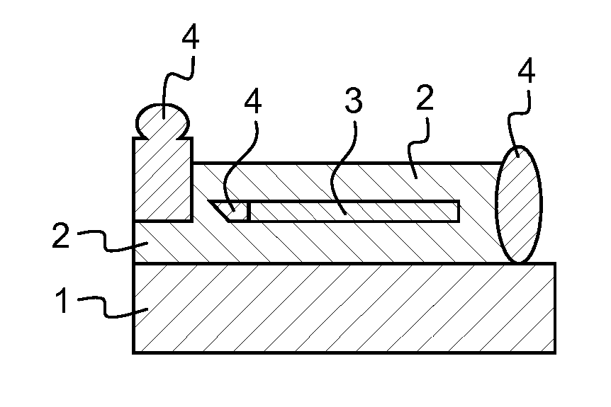
[0034]In some embodiments, at least one of the distinct components presents a concave shape along the direction of the thickness of the three dimensional guided wave photonic device.

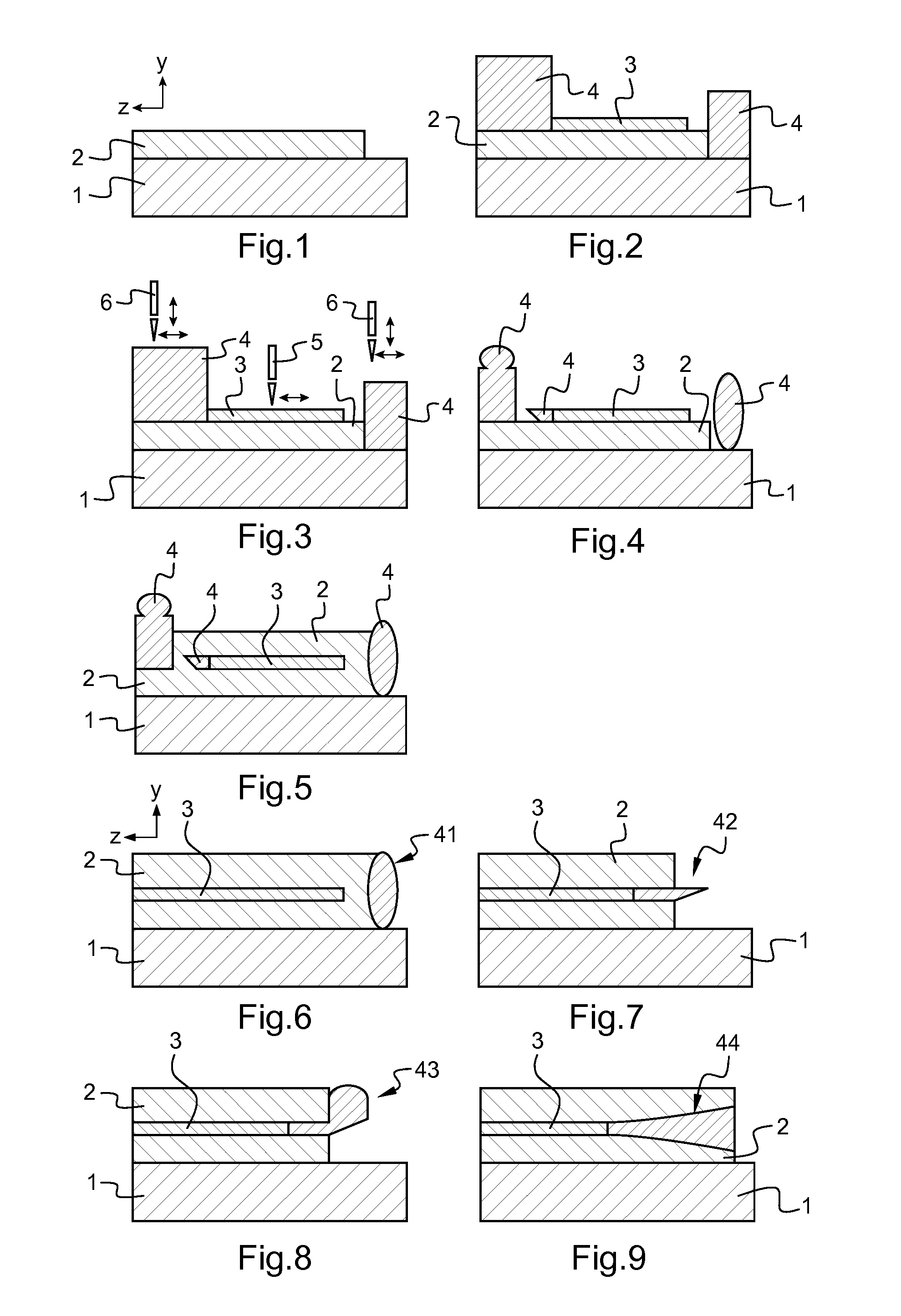
[0035]In some embodiments, the manufacturing is performed by hybrid direct laser writing including a first beam to perform the direct laser writing involving polymerization by two-photon absorption, to build three dimensional components, and a second beam, distinct ...


PUM


Abstract

A method of manufacturing a three dimensional photonic device by two photon absorption polymerization. The method includes several stages, including direct laser writing involving polymerization by two-photon absorption to manufacture a three dimensional photonic device integrating at least two distinct micro-optical components having two optical functions and being aligned with each other so that optical signal can be transmitted from one of said distinct components to the other. The distinct components are built at a same stage of the process flow to improve their relative alignment by direct laser writing involving polymerization by two-photon absorption.

Description

CROSS-REFERENCE TO RELATED APPLICATION [0001]This application claims priority under 35 U.S.C. §119 from United Kingdom (GB) Patent Application No. 1209083.3 filed May 24, 2012, the entire contents of which are incorporated herein by reference.TECHNICAL FIELD[0002]The invention relates to methods of manufacturing a three dimensional photonic device including several distinct micro-optical components, which can be very different from one another, in an efficient and reliable way.BACKGROUND[0003]When manufacturing a three dimensional photonic device including several distinct micro-optical components, the more different the micro-optical components are from one another, the more difficult it is to integrate them in a single device, in an efficient and reliable way.[0004]The integration of optical waveguides with free-space micro-optical components and micromechanical structures is a major technical problem because high positioning accuracy, cost efficiency, high yield and reliability h...

Claims


Application Information

Patent Timeline
Patent Type & Authority Applications(United States)
IPC IPC(8): G02B6/138
CPCG02B6/138G02B6/12002G02B6/12004
Inventor LA PORTA, ANTONIOOFFREIN, BERT JSOGANCI, IBRAHIM MURAT
Owner GLOBALFOUNDRIES INC
Why Eureka
Try Eureka