Method for removing native oxide and associated residue from a substrate

a technology of native oxide and associated residues, which is applied in the direction of cleaning processes and apparatus, chemical instruments and processes, electric discharge tubes, etc., can solve the problems of affecting the quality of native oxide, difficulty in subsequent fabrication processes, and the general undesirable effect of native oxide layers

Inactive Publication Date: 2013-11-28
APPLIED MATERIALS INC
View PDF1 Cites 4 Cited by
  • Summary
  • Abstract
  • Description
  • Claims
  • Application Information

AI Technical Summary

Problems solved by technology

The presence of native oxides and other contaminants such as etch residue within these small apertures is highly undesirable, contributing to void formation during subsequent metalization of the aperture and increasing the electrical resistance of the interconnect feature.
In addition, native oxides may result from contamination during etching processes.
Native oxide films are usually very thin, for example between 5-20 angstroms, but thick enough to cause difficulties in subsequent fabrication processes.
Therefore, a native oxide layer is typically undesirable and needs to be removed prior to subsequent fabrication processes.
For example, a particular problem arises when native silicon oxide films are formed on exposed silicon containing layers, especially during processing of metal oxide silicon field effect transistor (MOSFET) structures.
Silicon oxide films are electrically insulating and are undesirable at interfaces with contact electrodes or interconnecting electrical pathways because they cause high electrical contact resistance.
Native silicon oxide films at the interface between the silicon substrate and the deposited metal reduce the compositional uniformity of the silicide layer by impeding the diffusional chemical reaction that forms the metal silicide during anneal.
This results in lower substrate yields and increased failure rates due to overheating at the electrical contacts.
Sputter etch processes have been used to reduce contaminants, but are generally only effective in large features or in small features having aspect ratios less than about 4:1.
In addition, sputter etch processes can damage delicate silicon layers by physical bombardment.
Wet etch processes utilizing hydrofluoric acid are used to remove native oxides, but are less effective in smaller features with aspect ratios exceeding 4:1.
This is because the aqueous solution has difficulty penetrating and being removed from vias, contacts, or other small features formed on the substrate surface, resulting in incomplete removal of the native oxide film and subsequent contamination issues.
In high aspect ratio features, however, the thin film may not completely sublime, leaving an unwanted residue on the substrate.
Furthermore, water generated in the formation of the thin film may produce additional native oxide on the substrate.

Method used


Image

  • Method for removing native oxide and associated residue from a substrate
  • Method for removing native oxide and associated residue from a substrate
  • Method for removing native oxide and associated residue from a substrate

Examples


Embodiment Construction

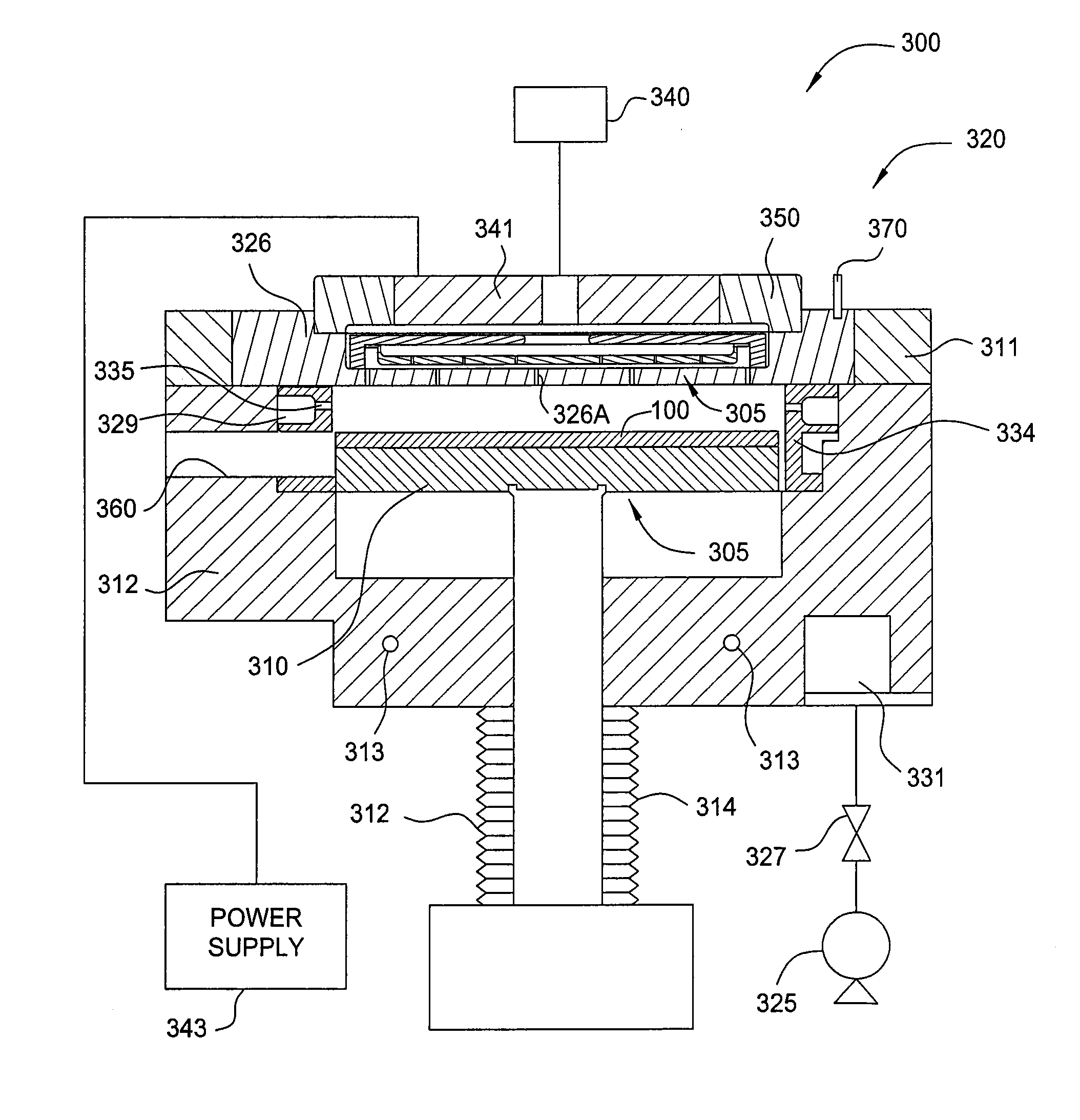
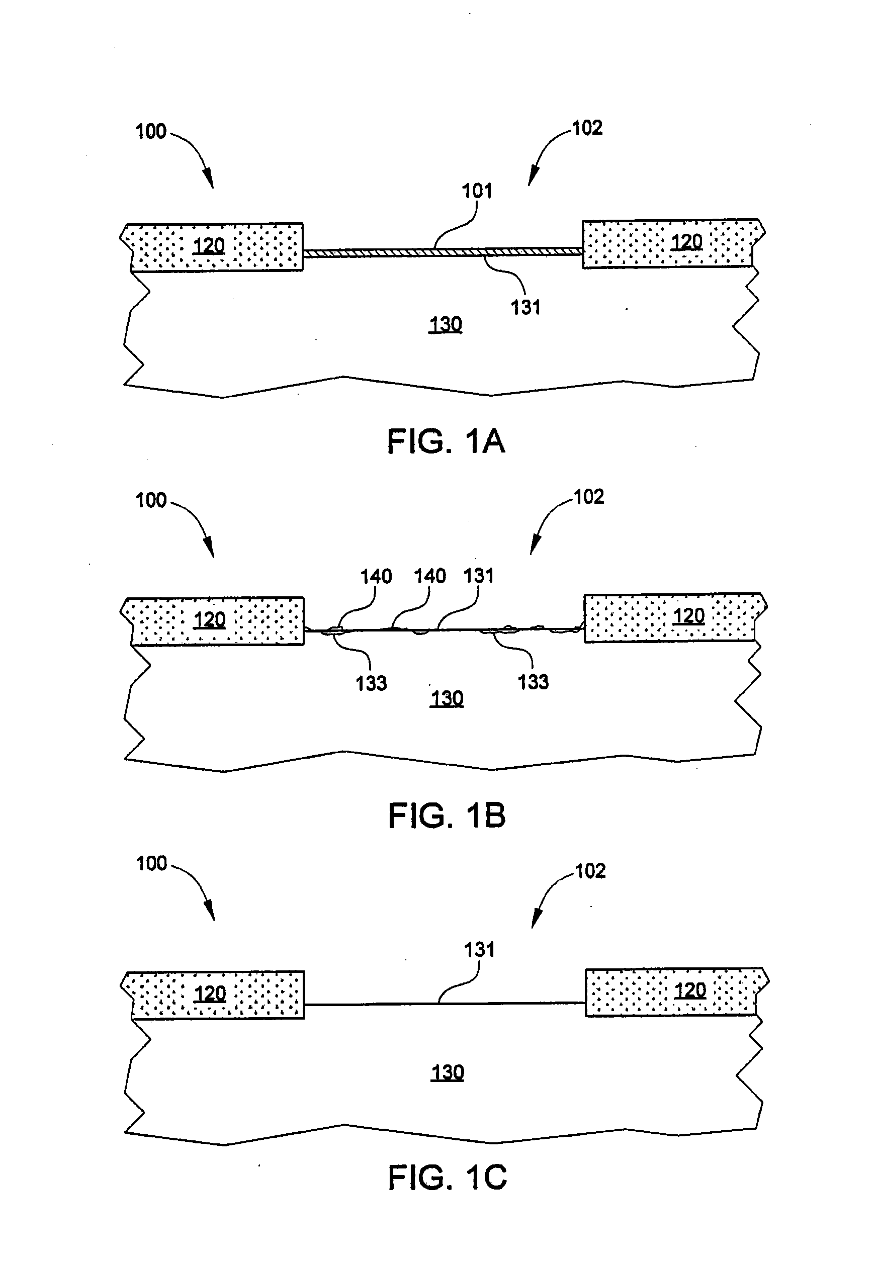
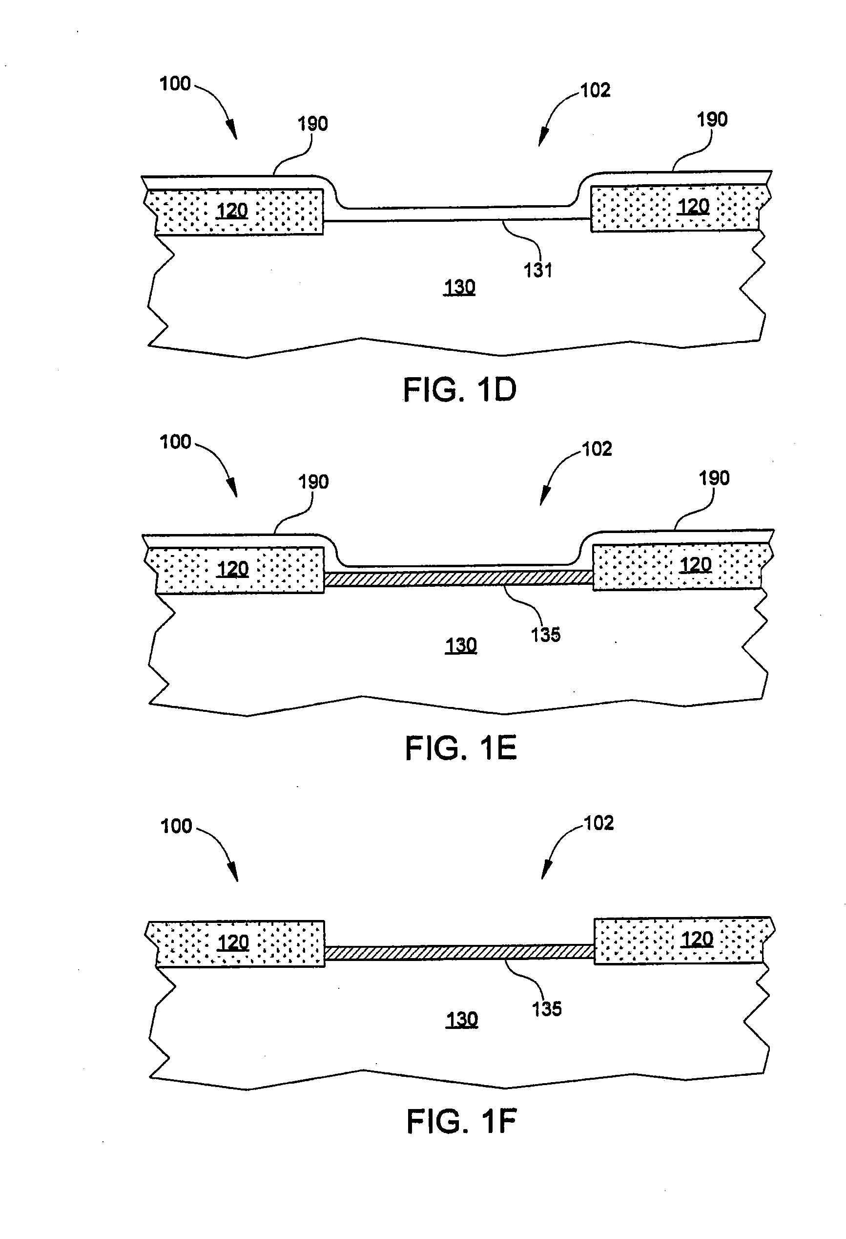
[0019]FIGS. 1A-1F are schematic cross-sectional views of a substrate surface treated according to embodiments of the invention. Substrate 100 may be a 200 or 300 mm silicon wafer, or any other substrate used to fabricate microelectronic devices and the like. Substrate 100 includes a bulk region 130 that may be a silicon-containing underlayer or may be the actual underlying bulk portion of substrate 100. As shown in FIG. 1A, substrate 100 includes a nitride layer 120 with an opening 102 formed therein to expose a surface 131 of bulk region 130. Nitride layer 120 may comprise silicon nitride (Si3N4) and / or other durable masking materials, and is deposited on bulk region 130 to protect bulk region 130 during oxide deposition and other fabrication processes. A native oxide layer 101 is formed in opening 102 of nitride layer 120 due to the exposure of surface 131 of bulk region 130 to either atmosphere or to one or more fabrication processes that cause native oxide layer 101 to form, suc...


PUM

PropertyMeasurementUnit
temperatureaaaaaaaaaa
plasma-generatingaaaaaaaaaa

Abstract

Native oxides and associated residue are removed from surfaces of a substrate by sequentially performing two plasma cleaning processes on the substrate in a single processing chamber. The first plasma cleaning process removes native oxide formed on a substrate surface by generating a cleaning plasma from a mixture of ammonia (NH3) and nitrogen trifluoride (NF3) gases, condensing products of the cleaning plasma on the native oxide to form a thin film that contains ammonium hexafluorosilicate ((NH4)2SiF6), and subliming the thin film off of the substrate surface. The second plasma cleaning process removes remaining residues of the thin film by generating a second cleaning plasma from nitrogen trifluoride gas. Products of the second cleaning plasma react with a few angstroms of the bare silicon present on the surface, forming silicon tetrafluoride (SiF4) and lifting off residues of the thin film.

Description

CROSS-REFERENCE TO RELATED APPLICATIONS[0001]This application is a continuation of U.S. patent application Ser. No. 13 / 480,091 (APPM / 15849), filed May 24, 2012, each of which is herein incorporated by reference.BACKGROUND OF THE INVENTION[0002]1. Field of the Invention[0003]Embodiments of the present invention relate generally to semiconductor substrate processing and, more particularly, to systems and methods for cleaning native oxide and associated residue from a substrate.[0004]2. Description of the Related Art[0005]In the microfabrication of integrated circuits and other devices, electrical interconnect features, such as contacts, vias, and lines, are commonly constructed on a substrate using high aspect ratio apertures formed in a dielectric material. The presence of native oxides and other contaminants such as etch residue within these small apertures is highly undesirable, contributing to void formation during subsequent metalization of the aperture and increasing the electri...

Claims


Application Information

Patent Timeline
Patent Type & Authority Applications(United States)
IPC IPC(8): H01L21/768H01L21/02
CPCH01L21/768H01L21/02057H01L21/0206H01J37/32082H01L21/28518H01L21/743H01L21/02063H01L21/28556H01L21/28568
Inventor ZHENG, BOSUNDARRAJAN, ARVINDFU, XINYU
Owner APPLIED MATERIALS INC
Why Eureka
Try Eureka