
Nitrogen profile engineering in nitrided high dielectric constant films

Inactive Publication Date: 2008-04-03
TOKYO ELECTRON LTD
View PDF34 Cites 373 Cited by
  • Summary
  • Abstract
  • Description
  • Claims
  • Application Information

AI Technical Summary

Benefits of technology

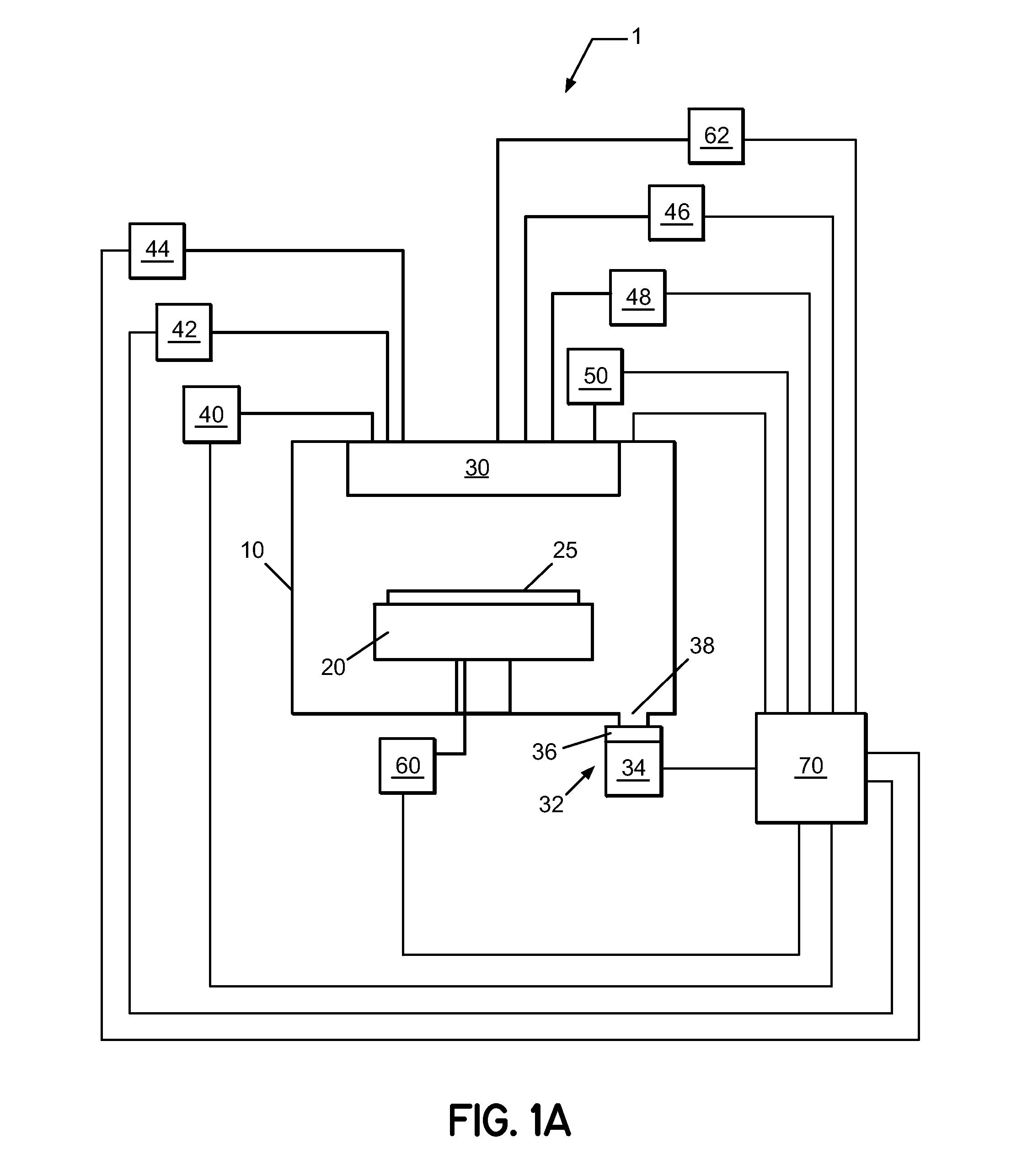
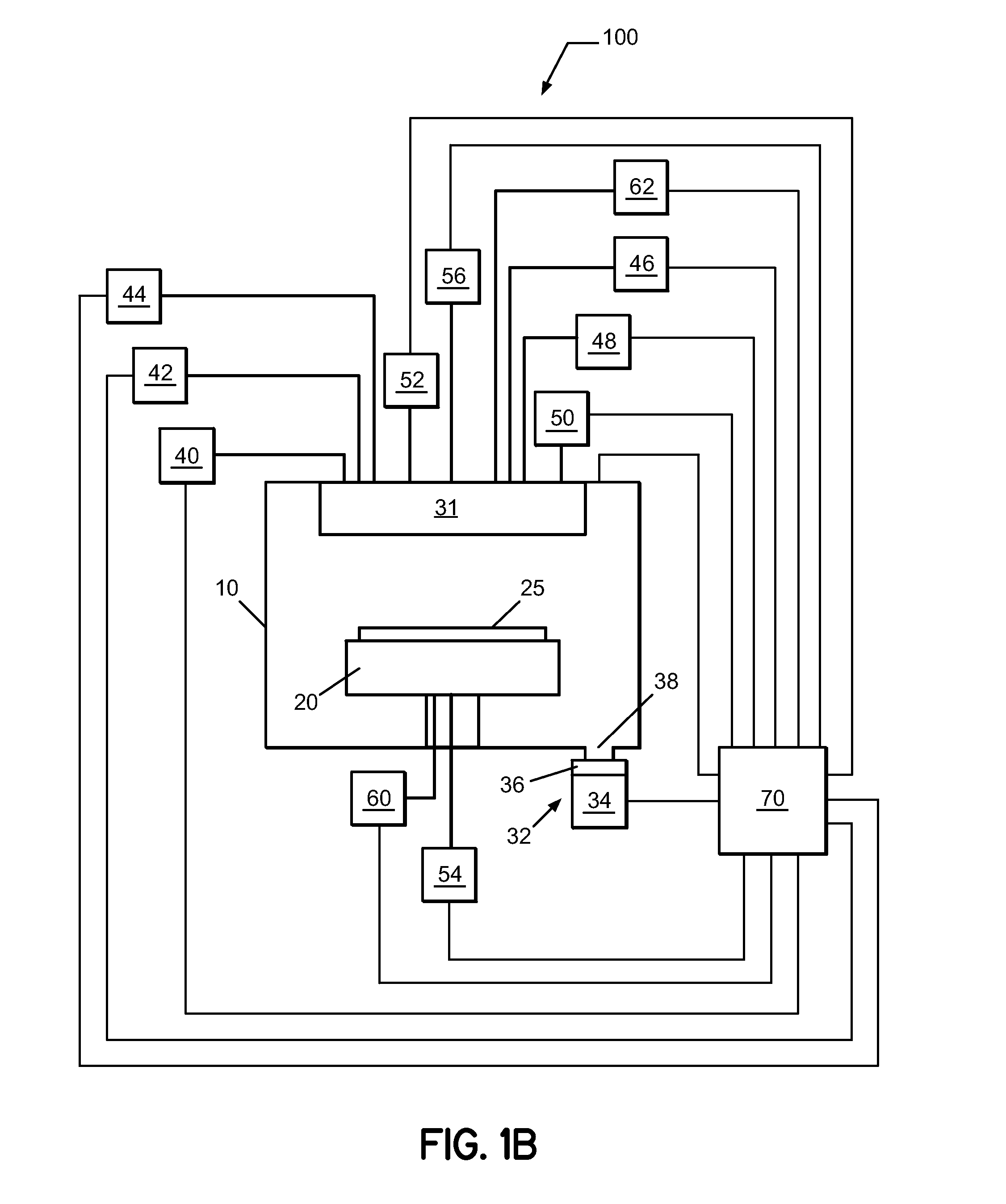
[0007]Embodiments of the invention provide a method for forming nitrided high-k films having a nitrogen gradient across a thickness of the films. The nitrided high-k films may be deposited by atomic layer deposition (ALD) or plasma-enhanced ALD (PEALD). For example, the nitrided high-k films may be used in advanced semiconductor devices that include capacitors and transistors.
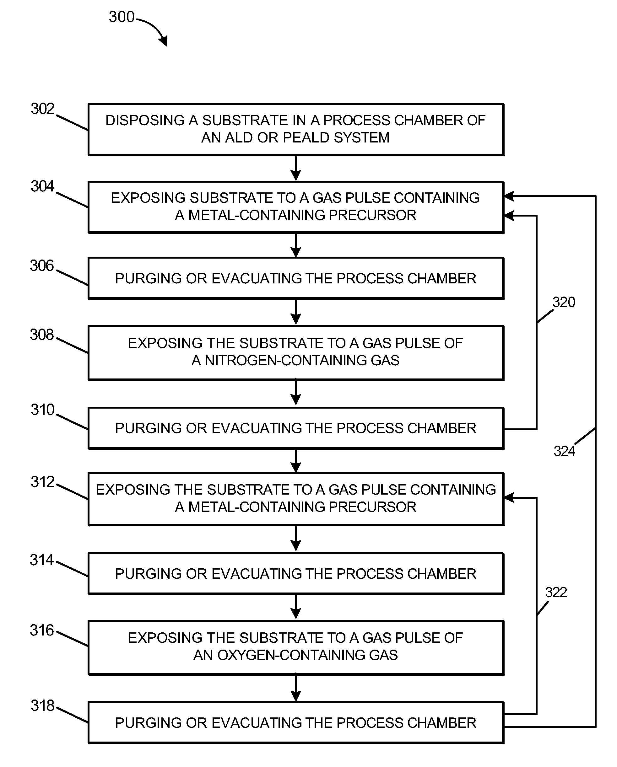
[0008]According to one embodiment of the invention, the method includes disposing a substrate in a process chamber, and forming a nitrided high-k film on the substrate by a) depositing a nitrogen-containing film, and b) depositing an oxygen-containing film, where steps a) and b) are performed, in any order, any number of times

Problems solved by technology

However, as the thickness of the ultra-thin SiON films is further reduced, acceptable leakage currents cannot be maintained.
However, many high-k dielectric materials under evaluation suffer from various problems, such as film crystallization during anneals, growth of interfacial layers during film deposition and further processing, high density of interface traps, reduced channel mobility, reaction with poly-silicon gates, and Fermi level pinning with metal gates.
Furthermore, many high-k dielectric materials have dielectric constants that are lower than is desired for many advanced semiconductor devices.
Nitrogen-incorporation into high-k dielectric materials is commonly performed by post-deposition plasma processing but this can be more difficult than for conventional silicon-based dielectric materials and may cause plasma damage of the high-k dielectric material.

Method used


Image

  • Nitrogen profile engineering in nitrided high dielectric constant films
  • Nitrogen profile engineering in nitrided high dielectric constant films
  • Nitrogen profile engineering in nitrided high dielectric constant films

Examples


example 1

[0097]Formation of a Bottom Nitrided Hafnium Based High-k Film

[0098]A hafnium based nitrogen-containing film having a thickness between about 5 angstrom and about 10 angstrom is deposited onto a substrate at a substrate temperature between 150° C. and 350° C. using alternating pulses of TEMAH and ammonia. Next, a hafnium based oxygen-containing film having a thickness between about 10 angstrom and about 30 angstrom is deposited onto the nitrogen-containing film at a substrate temperature between 150° C. and 350° C. using alternating pulses of TEMAH and mixture of ozone / oxygen. The ozone concentration in the mixture may be between 50 and 250 g / m3. Oxygen incorporation into the nitrogen-containing film during deposition of the oxygen-containing film oxidizes at a least a portion of the thickness of the nitrogen-containing film. In addition, oxygen incorporation may occur from the oxygen-containing film. Optionally, further oxygen incorporation may be achieved by additional ozone / oxyge...

example 2

[0099]Formation of a Middle Nitrided Hafnium Based High-k Film

[0100]A first (bottom) hafnium based oxygen-containing film having a thickness between about 5 angstrom and about 10 angstrom is deposited onto the substrate using alternating pulses of TEMAH and mixture of ozone / oxygen. Next, a (middle) hafnium based nitrogen-containing film having a thickness between about 10 angstrom and about 20 angstrom may be deposited onto the first hafnium based oxygen-containing film using alternating pulses of TEMAH and ammonia. Next, a second (top) hafnium based oxygen-containing film is deposited onto the nitrogen-containing film. The second hafnium based oxygen-containing film may have the same thickness as the first hafnium based oxygen-containing film. Oxygen incorporation into the nitrogen-containing film during deposition of the second oxygen-containing film oxidizes at least a portion of the thickness of the nitrogen-containing film. In addition, oxygen incorporation may occur from the f...

example 3

[0101]Formation of a Top Nitrided Hafnium Based High-k Film

[0102]A hafnium based oxygen-containing film having a thickness between about 10 angstrom and about 30 angstrom is deposited onto the substrate using alternating pulses of TEMAH and mixture of ozone / oxygen. A hafnium based nitrogen-containing film having a thickness between about 5 angstrom and about 10 angstrom is deposited onto the hafnium based oxygen-containing film using alternating pulses of TEMAH and ammonia. Oxygen incorporation into the nitrogen-containing film may occur from the oxygen-containing film. Optionally, further oxygen incorporation may be achieved by additional ozone / oxygen exposure prior to, during, or after deposition of the nitrogen-containing film.


PUM

PropertyMeasurementUnit
Thicknessaaaaaaaaaa
Dielectric constantaaaaaaaaaa

Abstract

A method of forming a nitrided high-k film by disposing a substrate in a process chamber and forming the nitrided high-k film on the substrate by a) depositing a nitrogen-containing film, and b) depositing an oxygen-containing film, wherein steps a) and b) are performed in any order, any number of times, so as to oxidize at least a portion of the thickness of the nitrogen-containing film. The oxygen-containing film and the nitrogen-containing film contain the same one or more metal elements selected from alkaline earth elements, rare earth elements, and Group IVB elements of the Periodic Table, and optionally aluminum, silicon, or aluminum and silicon. According to one embodiment, the method includes forming a nitrided hafnium based high-k film. The nitrided high-k film can be formed by atomic layer deposition (ALD) or plasma-enhanced ALD (PEALD).

Description

CROSS REFERENCE TO RELATED APPLICATION[0001]This application is related to co-pending U.S. patent application Ser. No. ______, filed on even date herewith and entitled “SEMICONDUCTOR DEVICES CONTAINING NITRIDED HIGH DIELECTRIC CONSTANT FILMS,” and copending U.S. patent application Ser. No. 11 / 278,396 and entitled “METHOD OF FORMING MIXED RARE EARTH OXYNITRIDE AND ALUMINUM OXYNITRIDE FILMS BY ATOMIC LAYER DEPOSITION.” The entire contents of these applications are herein incorporated by reference in their entirety.FIELD OF INVENTION[0002]The present invention relates to a method of forming high dielectric constant materials for semiconductor devices, and more particularly to a method of forming nitrided high dielectric constant films having a nitrogen gradient across a thickness of the films.BACKGROUND OF THE INVENTION[0003]Traditionally, thermal silicon oxide (SiO2) films, grown thermally from Si substrates, have been used as gate dielectric films in integrated circuits. More recentl...

Claims


Application Information

Patent Timeline
IPC IPC(8): C23C16/00H05H1/24
CPCC23C16/308C23C16/45542C23C16/45529
Inventor CLARK, ROBERT D.
Owner TOKYO ELECTRON LTD
Learn More