Method of etching high aspect ratio features in a dielectric layer

a technology of dielectric layer and high aspect ratio, which is applied in the direction of basic electric elements, semiconductor/solid-state device manufacturing, electric apparatus, etc., can solve the problems of har etching being polymer management, presenting greater challenges for the har etch process, and smaller width features with higher aspect ratios are more susceptible to the effects of polymer build-up

Inactive Publication Date: 2013-05-16
APPLIED MATERIALS INC
View PDF5 Cites 397 Cited by
  • Summary
  • Abstract
  • Description
  • Claims
  • Application Information

AI Technical Summary

Problems solved by technology

The widths of etched features decrease with scaling while the corresponding aspect ratios increase, thereby presenting greater challenges for the HAR etch process.
One of the major challenges in HAR etching is polymer management.
Smaller width features with higher aspect ratios are more susceptibl...

Method used


Image

  • Method of etching high aspect ratio features in a dielectric layer
  • Method of etching high aspect ratio features in a dielectric layer
  • Method of etching high aspect ratio features in a dielectric layer

Examples


Embodiment Construction

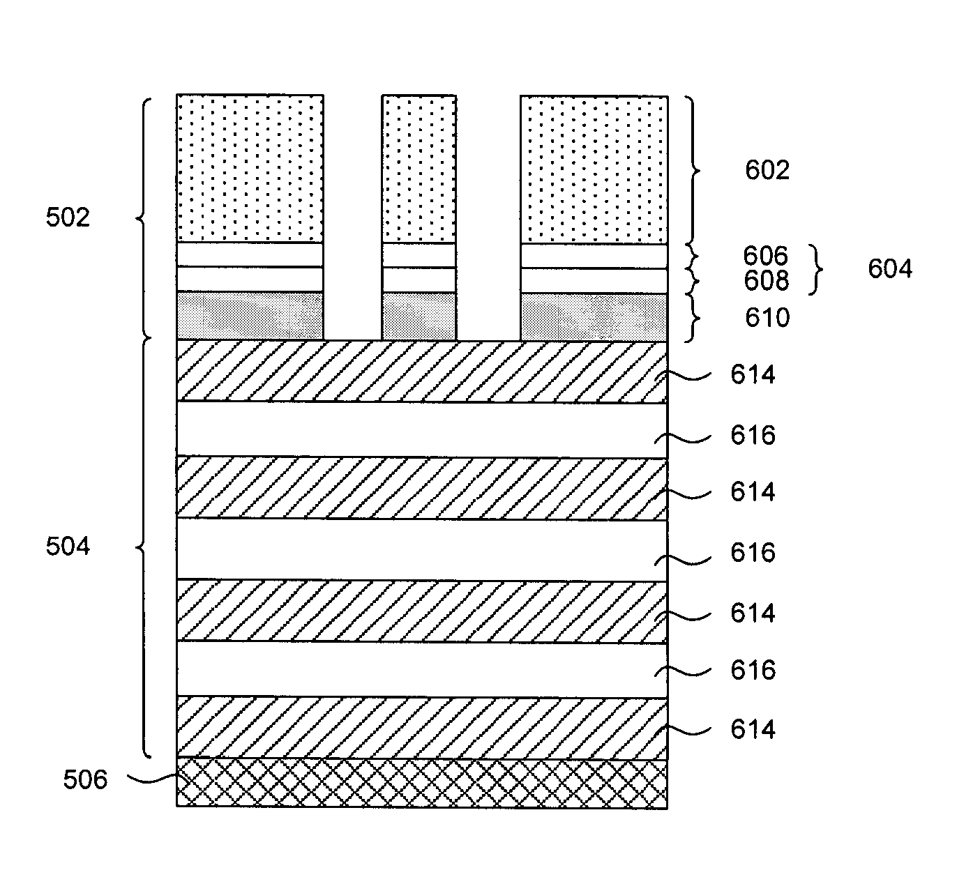
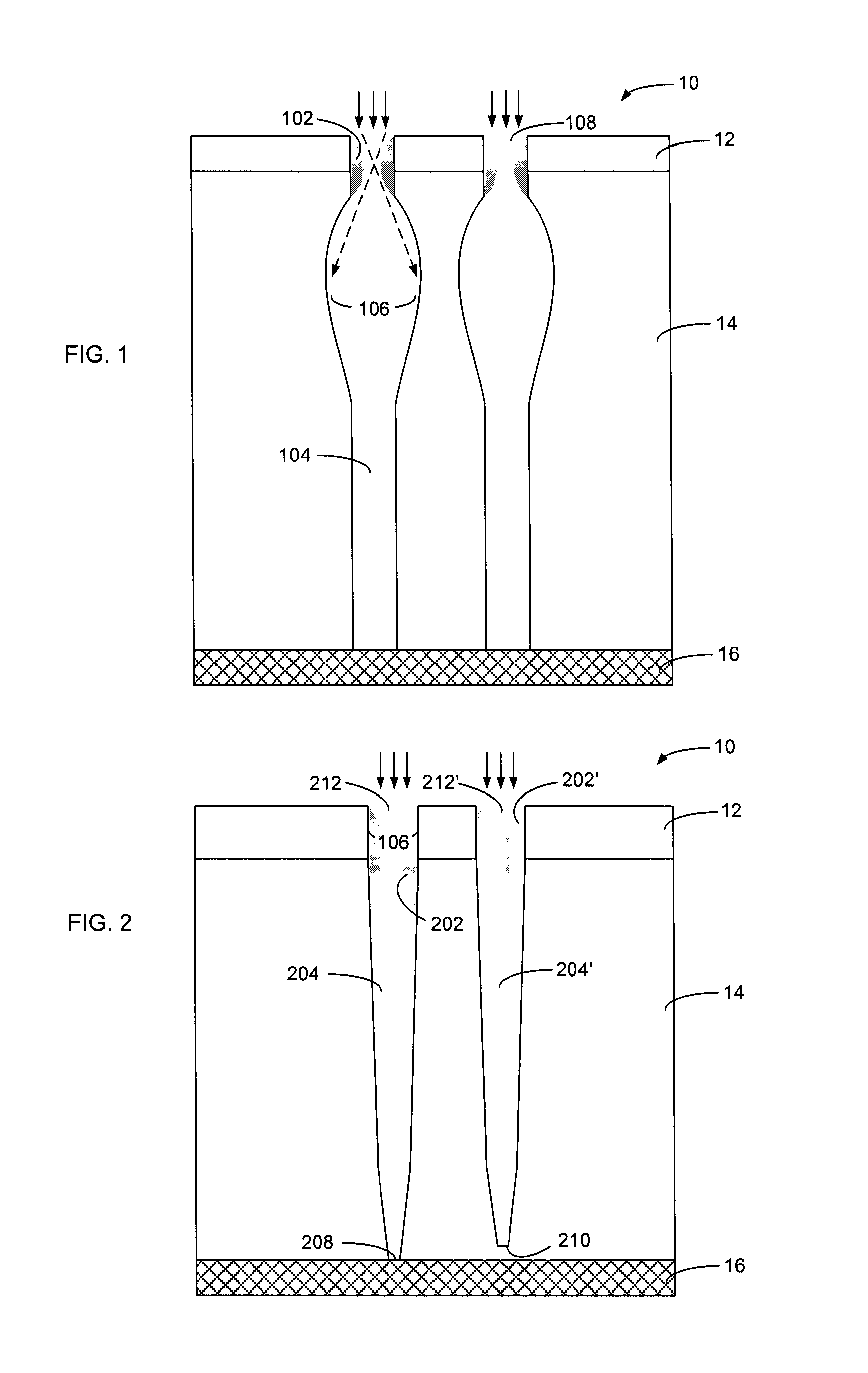
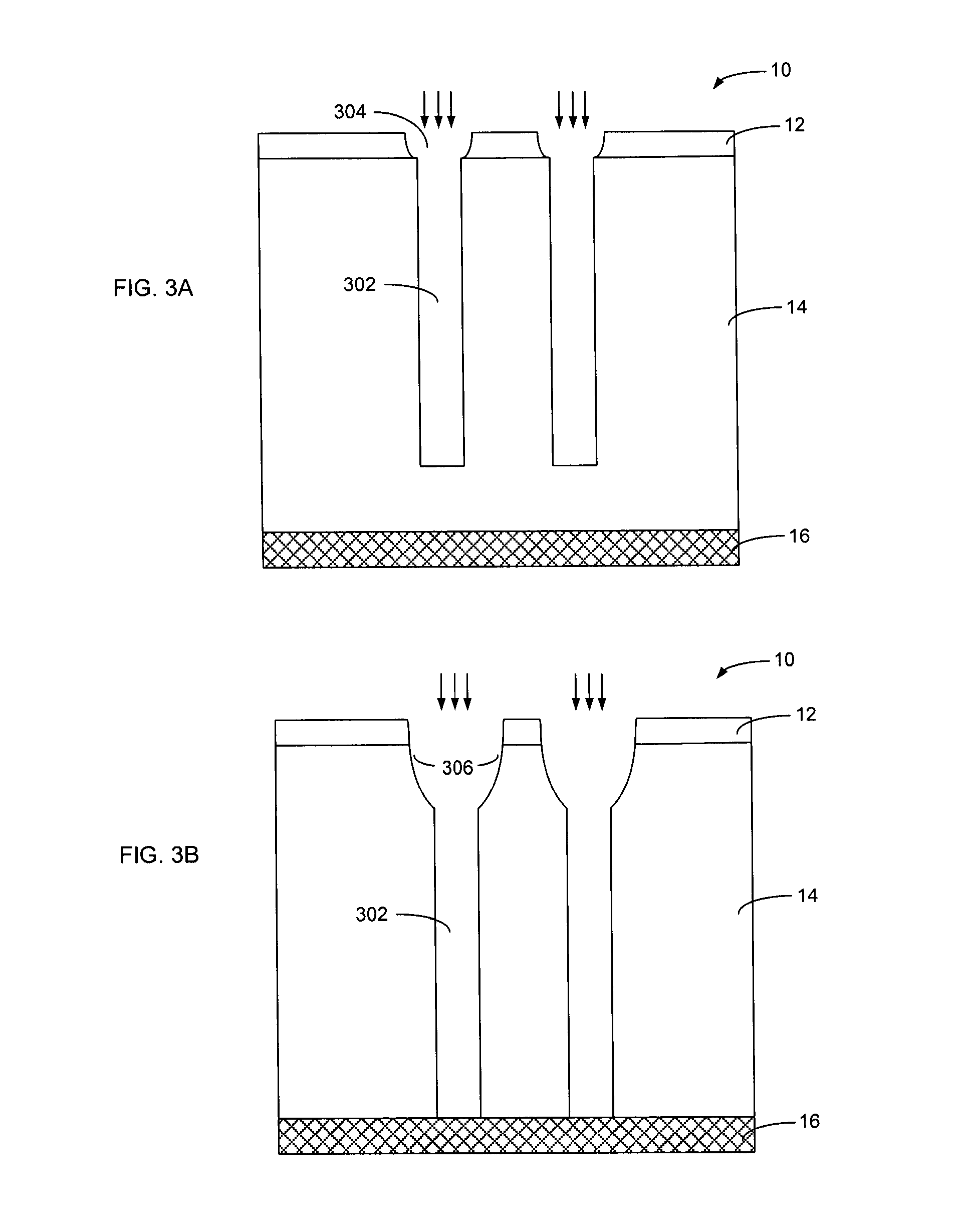
[0018]Methods of etching high aspect ratio (HAR) features in a dielectric layer are described. In the context of the current application, the term “high aspect ratio” (HAR) features refers to features with depth to width ratios of about 20:1 or more. In the following description, numerous details are set forth. It will be apparent, however, to one skilled in the art, that the present invention may be practiced without these specific details. In other instances, well-known aspects, such as photolithography patterning and development for mask formation, are not described in detail to avoid obscuring the present invention. Reference throughout this specification to “an embodiment” means that a particular feature, structure, function, or characteristic described in connection with the embodiment is included in at least one embodiment of the invention. Thus, the appearances of the phrase “in an embodiment” in various places throughout this specification are not necessarily referring to t...


PUM


Abstract

Methods of etching HAR features in a dielectric layer are described. In one embodiment, a substrate is provided into an etch chamber. The substrate has a patterned mask disposed on a dielectric layer formed thereon where the patterned mask has openings. A gas mixture is provided into the etch chamber, the gas mixture includes CO, O2, a fluorocarbon gas, and an optional inert gas. A plasma is formed from the gas mixture. Features are etched in the dielectric layer through the openings in the presence of the plasma

Description

CROSS-REFERENCE TO RELATED APPLICATIONS[0001]This application claims the benefit of and priority to U.S. Provisional Application No. 61 / 559,617, filed Nov. 14, 2011, the entire contents of which are hereby incorporated by reference herein.BACKGROUND[0002]1) Field[0003]This invention relates to a method of etching high aspect ratio features in a dielectric layer.[0004]2) Description of Related Art[0005]High aspect ratio (HAR) etching of features such as contacts holes and trenches in dielectric layers is a key process in integrated circuit (IC) fabrication. For example, etching high aspect ratio contacts (HARC) through dielectric layers is important in the formation of electrical interconnections between different conductive layers. In dynamic random access memory (DRAM) fabrication, HAR container structures are etched through dielectrics layers in the formation of stacked capacitors. In 3D vertical NAND application, etching HAR contacts and trenches in dielectric layers are also imp...

Claims


Application Information

Patent Timeline
IPC IPC(8): H01L21/3065
CPCH01L21/31116
Inventor KIM, JONG MUNDOAN, KENNY LINHLING, LIPAYYAPILLY, JAIRAJSHIMUZU, DAISUKENEMANI, SRINIVAS D.LILL, THORSTEN B.
Owner APPLIED MATERIALS INC
Why Eureka
Try Eureka