Method for plasma etching a dielectric layer

a dielectric layer and plasma etching technology, applied in the direction of basic electric elements, semiconductor/solid-state device manufacturing, electric apparatus, etc., can solve the problems of difficult to achieve high-aspect ratio structure formation and undesirable tapered profile of structures

Inactive Publication Date: 2005-03-03
APPLIED MATERIALS INC
View PDF14 Cites 77 Cited by
  • Summary
  • Abstract
  • Description
  • Claims
  • Application Information

AI Technical Summary

Problems solved by technology

However, such one-step etch processes typically have a low etch selectively between the material of the etch mask and the dielectric material being etched so that formation of the high aspect ratio structures are difficult to achieve.
Additionally, polymer by-products from the etch process may accumulate on sidewalls of the structures during the etch process, producing structures having undesirable tapered profiles.

Method used


Image

  • Method for plasma etching a dielectric layer
  • Method for plasma etching a dielectric layer
  • Method for plasma etching a dielectric layer

Examples


Embodiment Construction

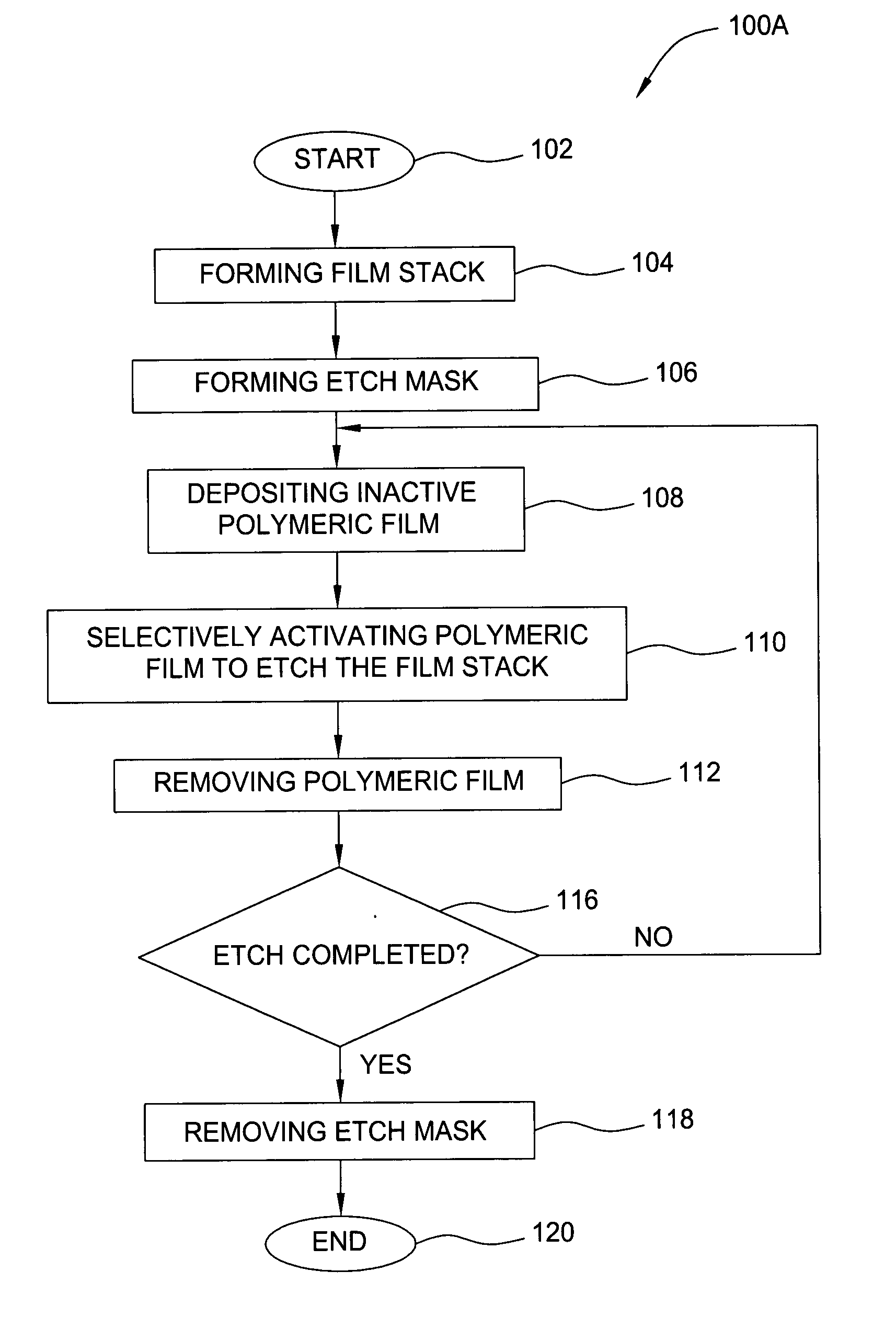
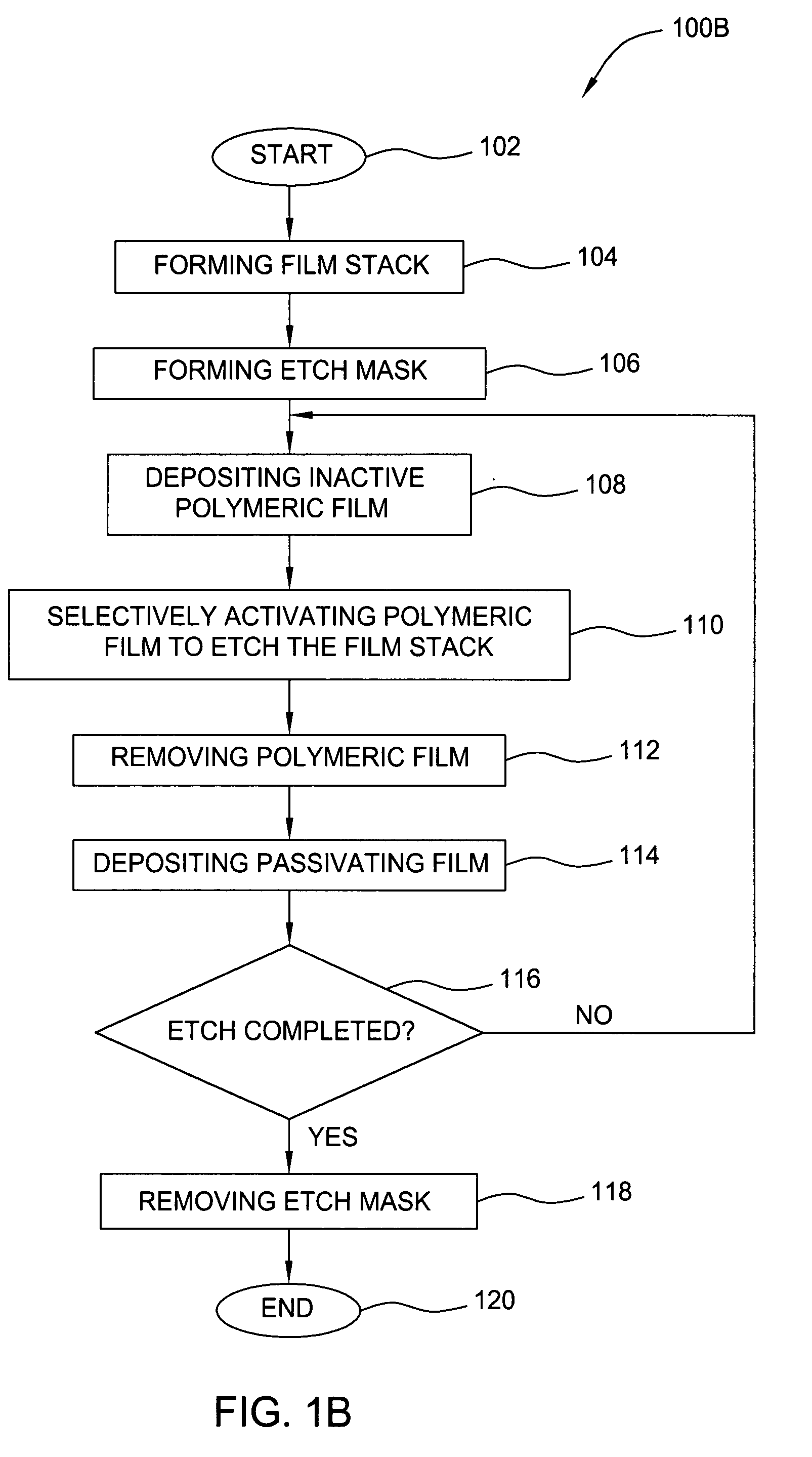
[0015] The present invention is a method of etching a structure in a layer of a dielectric material formed on a substrate, e.g., a silicon (Si) wafer. The layer may comprise at least one film of an oxide or oxynitride material, e.g., silicon dioxide (SiO2), silicon oxynitride (SiNXOY, where x and y are integers), and the like. Herein the terms “wafer” and “substrate” are used interchangeably.

[0016] In one application, the method is used to form structures such as trenches, vias, and the like having a smallest width in a plan view of about 0.1 to 20 μm and a ratio of a height of the structure to the width of about 5 to 50. Such structures are referred to herein as high aspect ratio (AR) structures. In other applications, the method may be used to form low AR structures, such as isolated lines, arrayed waveguides, and the like.

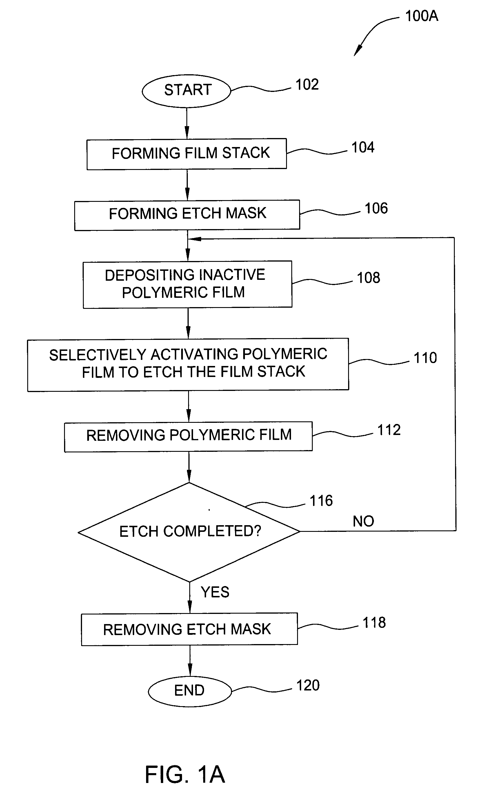
[0017]FIGS. 1A-1D depict, respectively, flow diagrams of exemplary embodiments 100A-100D of the invention during fabrication of an illustrative high aspect ra...


PUM


Abstract

A method of etching a dielectric layer formed on a substrate including a sequence of processing cycles, wherein each cycle comprises steps of depositing an inactive polymeric film, activating the film to etch the structure, and removing the film is disclosed. In one embodiment, the method uses a fluorocarbon gas to form the polymeric film and a substrate bias to activate such film.

Description

BACKGROUND OF THE INVENTION [0001] 1. Field of the Invention [0002] The present invention generally relates to substrate processing systems. More specifically, the present invention relates to a method for performing an etch process in a substrate processing system. [0003] 2. Description of the Related Art [0004] Manufacturing of optical and opto-electronic devices typically comprises a number of processes having limited analogies to the fabrication of electronic integrated circuits on semiconductor substrates. Such processes may comprise forming a structure having a smallest width of about 1 to 20 μm and a high aspect ratio of about 5 to 50 (e.g., trench, via, and the like), as well as fabrication of a structure having the aspect ratio less than 5 (e.g., isolated line, arrayed waveguide, and the like). Herein the term “aspect ratio” refers to a height of the structure divided by its smallest width. Such structures are generally formed in an oxide or oxynitride dielectric layer, e.g...

Claims


Application Information

Patent Timeline
Patent Type & Authority Applications(United States)
IPC IPC(8): H01L21/033H01L21/311
CPCH01L21/0332H01L21/31144H01L21/31116H01L21/30655
Inventor MERRY, WALTER R.MAK, CECILIA Y.LAW, KAM S.
Owner APPLIED MATERIALS INC
Why Eureka
Try Eureka