Composite hard mask for the etching of nanometer size magnetic multilayer based device

a nanometer-size magnetic multi-layer, hard mask technology, applied in semiconductor devices, thin material processing, electrical equipment, etc., can solve the problems of limiting the further reduction of line width, unable to manufacture a very high density ic device as is required for spin torque mram applications, and electrical shorting in the device, so as to prevent electrical shorting

Active Publication Date: 2009-03-26
TAIWAN SEMICON MFG CO LTD
View PDF4 Cites 87 Cited by
  • Summary
  • Abstract
  • Description
  • Claims
  • Application Information

AI Technical Summary

Benefits of technology

[0019]In a less preferred embodiment, the middle metallic spacer is omitted and the first etch step comprising a fluorocarbon gas stops on the lower non-magnetic layer. In this case, the lower non-magnetic layer is considerably thicker than in

Problems solved by technology

A sloped profile can not only lead to electrical shorting issues but also limits further reduction of linewidth and makes it impossible to manufacture a very high density IC device as is required for applications such as spin torque MRAM.
However, as the MTJ cell/pitch dimensions shrink to about 100 nm or less as required for spin torque MRAMs, the MTJ shapes generated by a RIE process may not be able to withstand subsequent CMP processing and bit line via (BLV

Method used


Image

  • Composite hard mask for the etching of nanometer size magnetic multilayer based device
  • Composite hard mask for the etching of nanometer size magnetic multilayer based device
  • Composite hard mask for the etching of nanometer size magnetic multilayer based device

Examples


Embodiment Construction

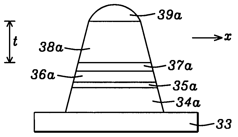
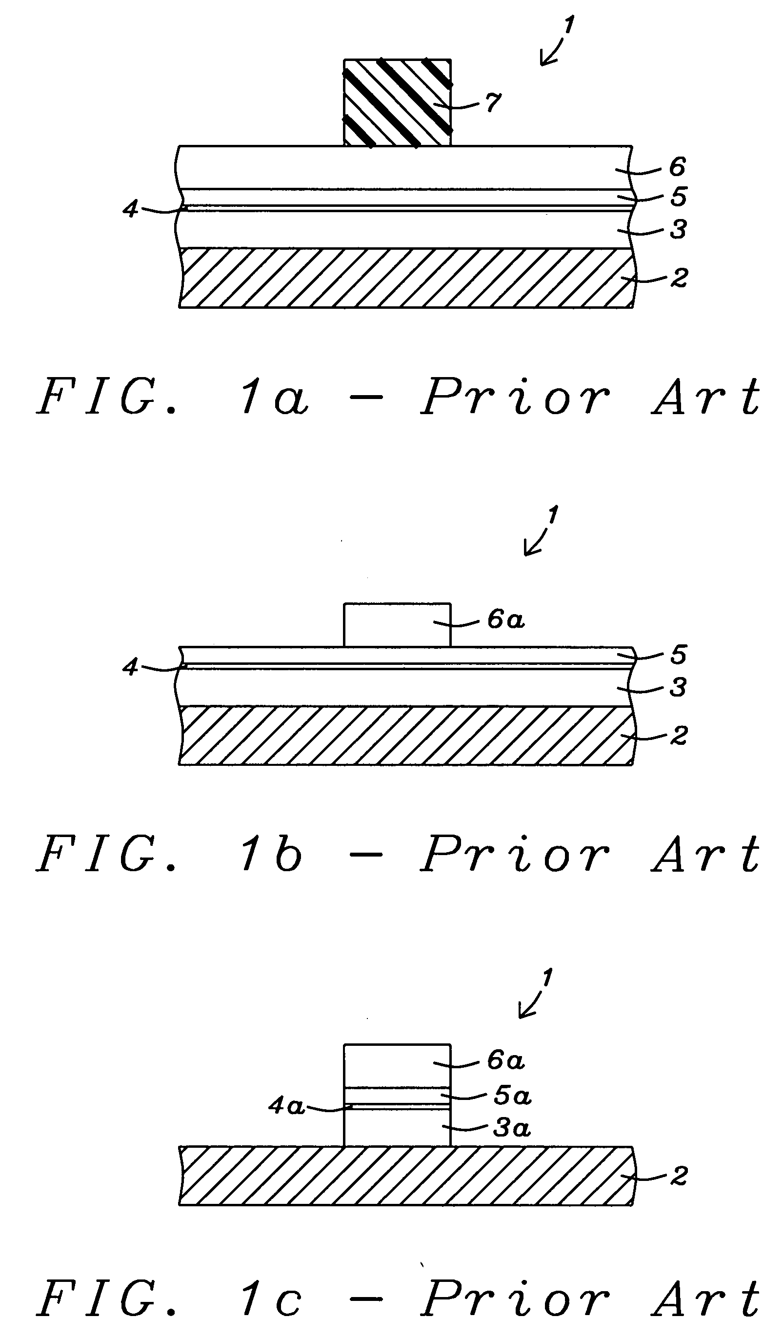
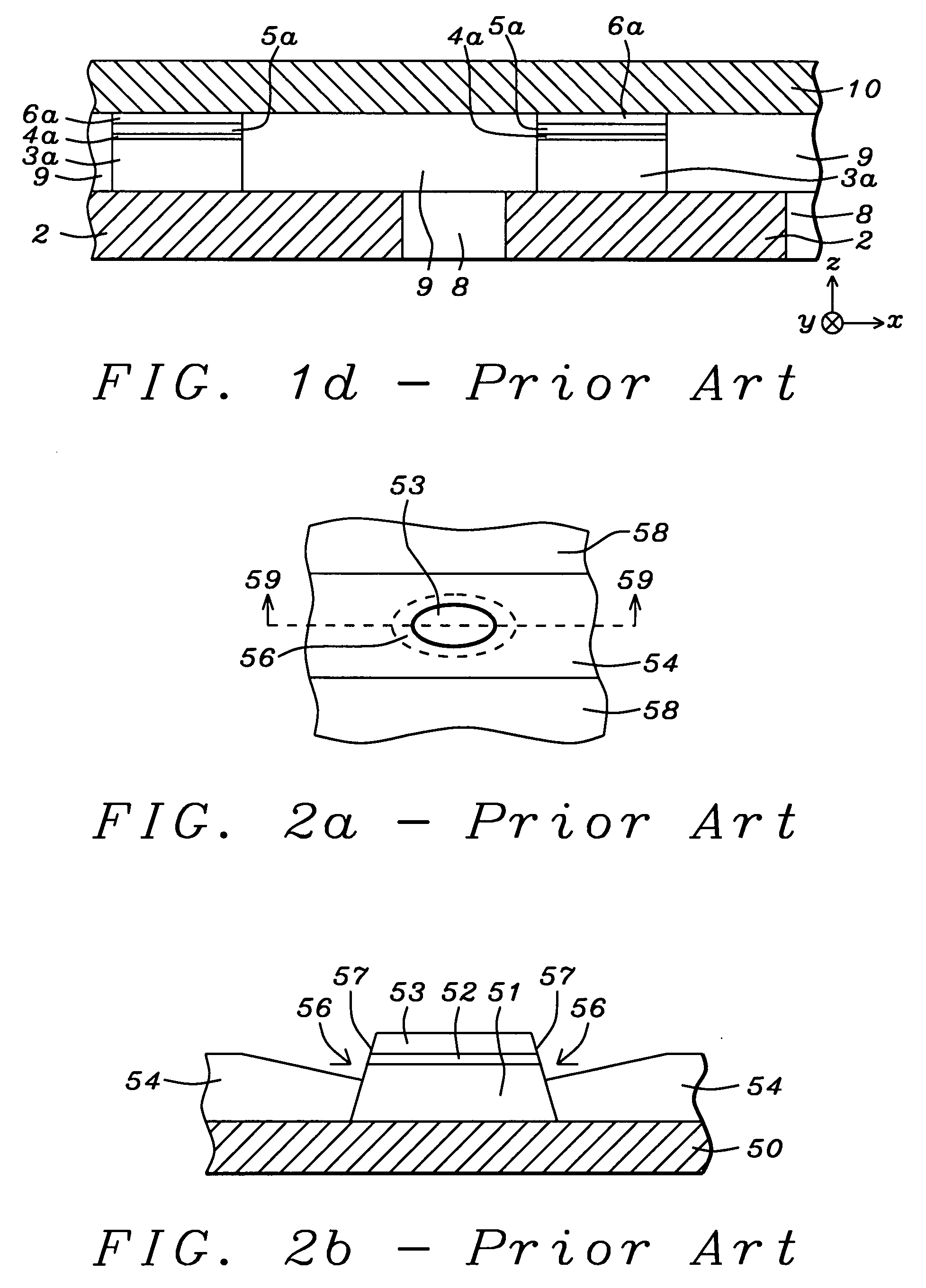
[0025]The present invention is a hard mask design and a method of using the hard mask to form MTJ cells having sub-100 nm resolution for advanced memory devices. The drawings are provided by way of example and are not intended to limit the scope of the invention. Further, the drawings are not necessarily drawn to scale and the relative sizes of various elements may differ from those in an actual device. Although a bottom spin valve MTJ structure is described in the exemplary embodiment, the present invention also encompasses other MTJ configurations such as top spin valve and multi-layer spin valve structures. A related MTJ etching process has been disclosed by the inventors in MagIC patent application HMG07-026 which describes the formation of easy axis and hard axis dimensions in a MTJ cell by employing separate photolithography steps and is herein incorporated by reference in its entirety.

[0026]A method of fabricating a MTJ cell by employing a composite hard mask structure accord...


PUM


Abstract

A composite hard mask is disclosed that enables sub-100 nm sized MTJ cells to be formed for advanced devices such as spin torque MRAMs. The hard mask has a lower non-magnetic metallic layer such as Ru to magnetically isolate an overlying middle metallic spacer such as MnPt from an underlying free layer. The middle metallic spacer provides a height margin during subsequent processing to avoid shorting between a bit line and the MTJ cell in the final device. An upper conductive layer may be made of Ta and is thin enough to allow a MTJ pattern in a thin overlying photoresist layer to be transferred through the Ta during a fluorocarbon etch without consuming all of the photoresist. The MTJ pattern is transferred through the remaining hard mask layers and underlying MTJ stack of layers with a second etch step using a C, H, and O etch gas composition.

Description

RELATED PATENT APPLICATION[0001]This application is related to the following: Docket # HMG06-008 / 014, Ser. No. 11 / 528,877, filing date Sep. 28, 2006; and Docket # HMG07-026, Ser. No. ______, filing date ______, both assigned to a common assignee and herein incorporated by reference in their entirety.FIELD OF THE INVENTION[0002]The invention relates to a composite hard mask that facilitates the formation of a MTJ element and an etch sequence involving the hard mask that enables sub-100 nm sized MTJs to be formed with sufficient process window latitude for manufacturing and with sufficient height margin to allow a subsequent chemical mechanical polish (CMP) step to proceed with acceptable yield.BACKGROUND OF THE INVENTION[0003]Magnetoresistive Random Access Memory (MRAM), based on the integration of silicon CMOS with MTJ technology, is a major emerging technology that is highly competitive with existing semiconductor memories such as SRAM, DRAM, Flash, etc. A MRAM device is generally ...

Claims


Application Information

Patent Timeline
IPC IPC(8): H01L29/06H01L21/02
CPCY10T428/24736H01L43/12H10N50/01
Inventor XIAO, RONGFUTORNG, CHYU-JIUHZHONG, TOMKULA, WITOLDZHONG, ADAM
Owner TAIWAN SEMICON MFG CO LTD
Why Eureka
Try Eureka