Method for producing an aperture plate
- Summary
- Abstract
- Description
- Claims
- Application Information
AI Technical Summary
Benefits of technology
Problems solved by technology
Method used
Image
Examples
Embodiment Construction
[0033]The invention will be more clearly understood from the following description of some embodiments thereof, given by way of example only with reference to the accompanying drawings in which:
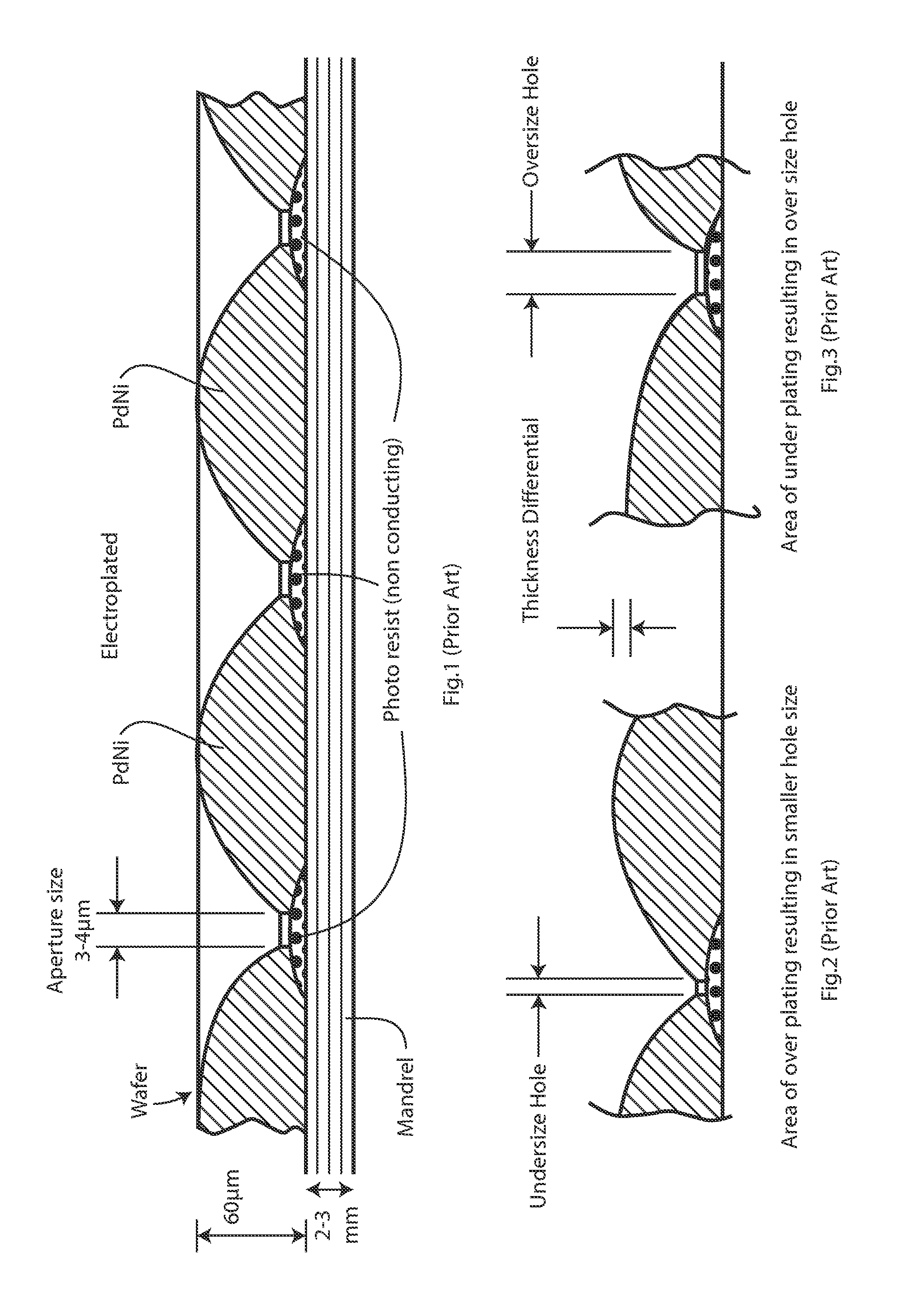
[0034]FIGS. 1 to 3 are cross-sectional diagrams outlining a prior art process as described above;
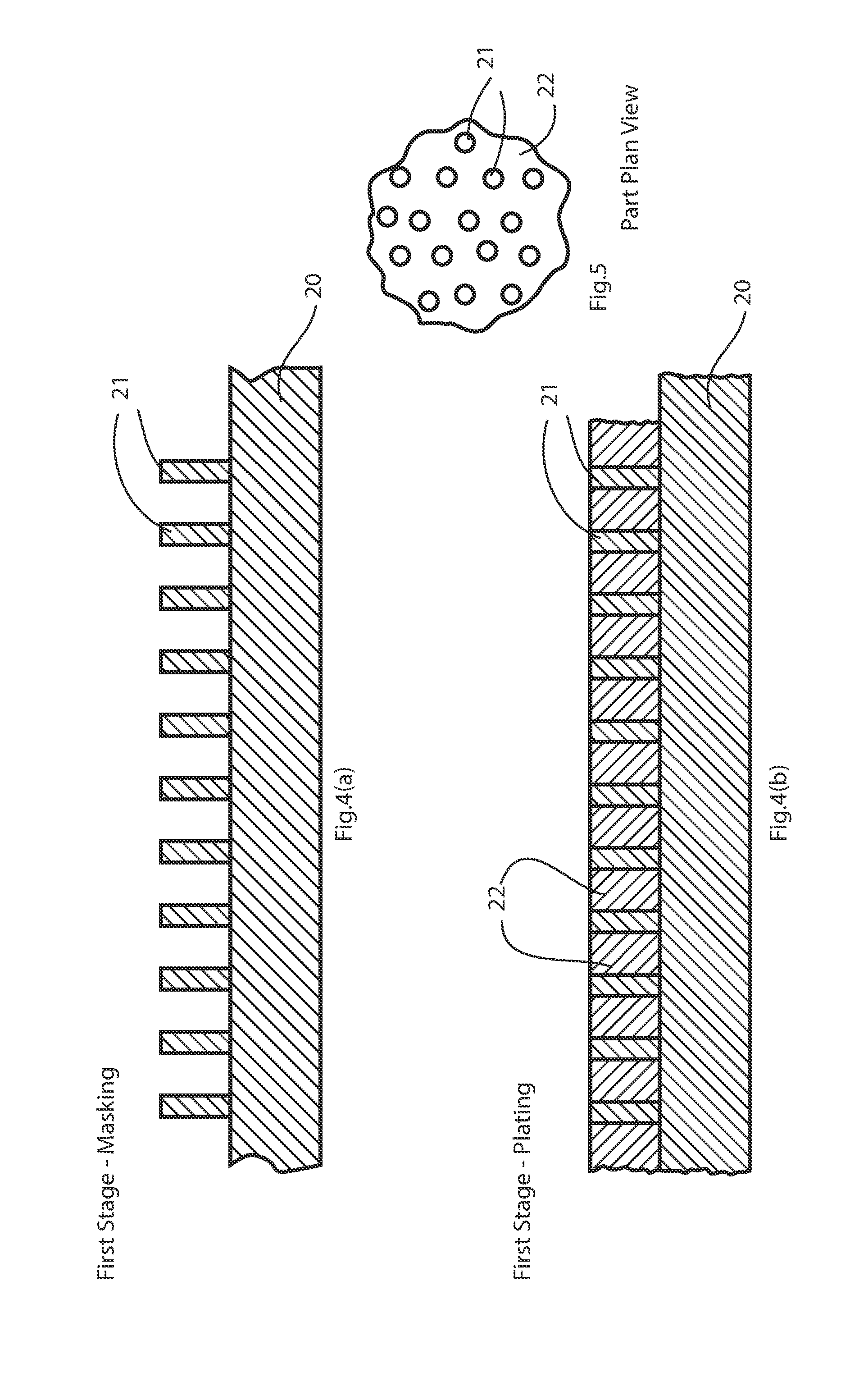
[0035]FIGS. 4(a) and 4(b) are cross-sectional views showing masking and plating steps for a first stage of the method, and FIG. 5 is a part plan view of the wafer for this stage;
[0036]FIGS. 6(a) and 6(b) are cross-sectional views showing a second masking and plating stage, and FIG. 7 is a plan view;
[0037]FIG. 8 is a cross-sectional view after resist removal;
[0038]FIG. 9 shows the wafer after punching to form the final aperture plate shape;
[0039]FIG. 10 is a plot of particle size vs. flow rate to illustrate operation of the aperture plate;
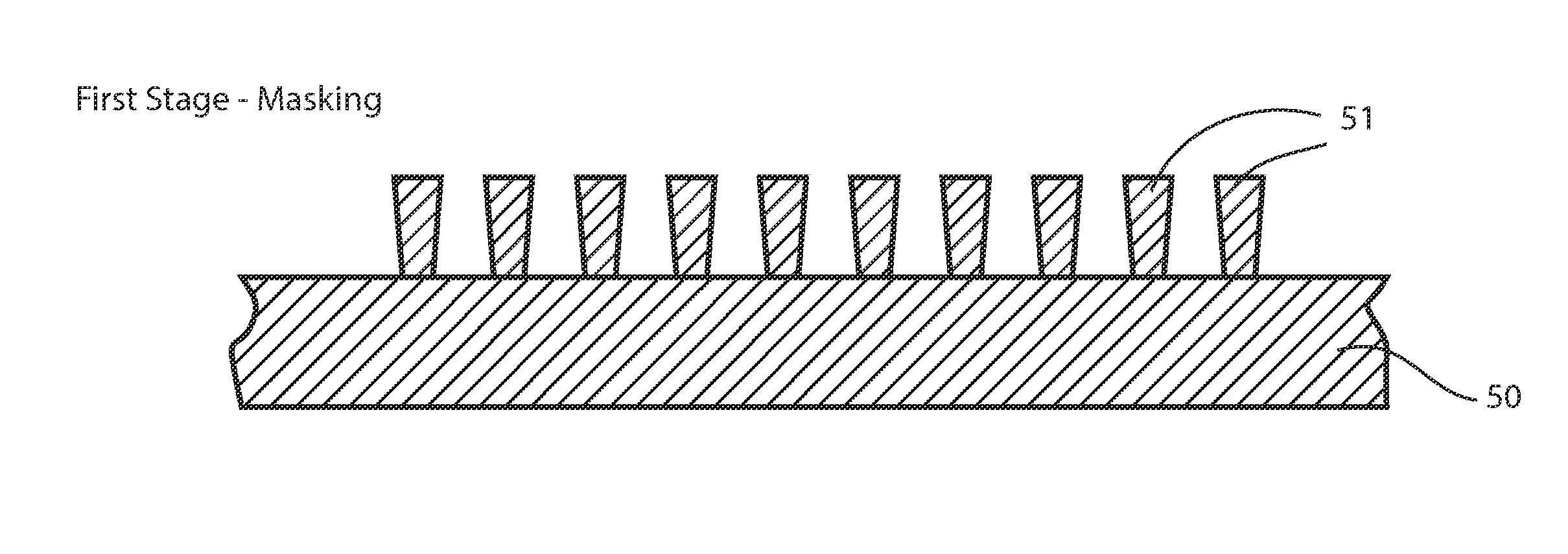
[0040]FIGS. 11(a), 11(b) and 12 are views equivalent to FIGS. 4(a), 4(b), and 5 for a second embodiment, in which the holes are tapered; and
[0041]FIGS. 13(a) and ...
PUM
| Property | Measurement | Unit |
|---|---|---|
| Fraction | aaaaa | aaaaa |
| Fraction | aaaaa | aaaaa |
| Fraction | aaaaa | aaaaa |
Abstract
Description
Claims
Application Information


