Display device and manufacturing method for same

a technology of display device and manufacturing method, which is applied in the direction of semiconductor devices, basic electric elements, electrical apparatus, etc., can solve the problems of data line being disconnected, display performance of display device significantly lowering, etc., and achieve high-reliability display device, reduce the number of multi-layer films and the number of etching steps, the effect of increasing the aperture ratio of pixels

Active Publication Date: 2013-12-19
JAPAN DISPLAY INC
View PDF7 Cites 20 Cited by
  • Summary
  • Abstract
  • Description
  • Claims
  • Application Information

AI Technical Summary

Benefits of technology

[0012]An object of the present invention is to solve the above-described problems and to provide a display device using an oxide semiconductor layer where the number of multilayer films and the number of steps in the etching can be reduced at the time of the manufacture of the display device, and in addition, the aperture ratio of the pixels can be increased, as well as to provide a manufacturing method for the same.
[0014]The present invention can provide a display device using an oxide semiconductor layer where the number of multilayer films and the number of etching steps can be reduced at the time of the manufacture of the display device, and the aperture ratio of the pixels can be increased, as well as a manufacturing method for the same, and thus, it becomes possible to provide a highly reliable display device.

Problems solved by technology

In addition, the pixel electrodes and the oxide semiconductor layer are structurally processed after the formation of the data lines, and therefore, the data lines may be dissolved or corroded by the etchant when the pixel electrodes and the oxide semiconductor layer are formed through etching, and as a result, the possibility of a data line being disconnected and the display performance of the display device significantly lowering increases.

Method used


Image

  • Display device and manufacturing method for same
  • Display device and manufacturing method for same
  • Display device and manufacturing method for same

Examples


Embodiment Construction

[0024]In the following, the preferred embodiments of the present invention are described in detail.

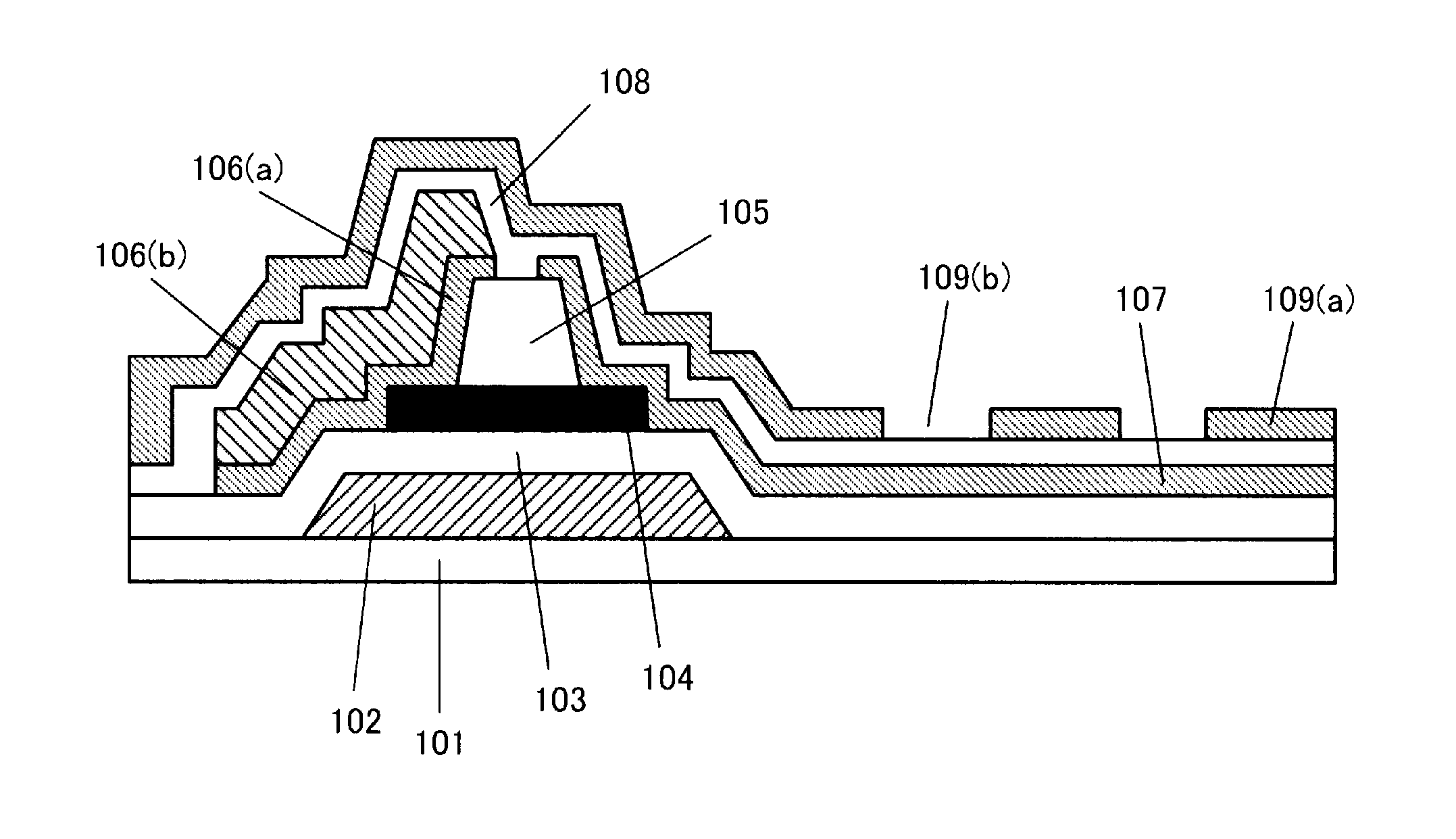
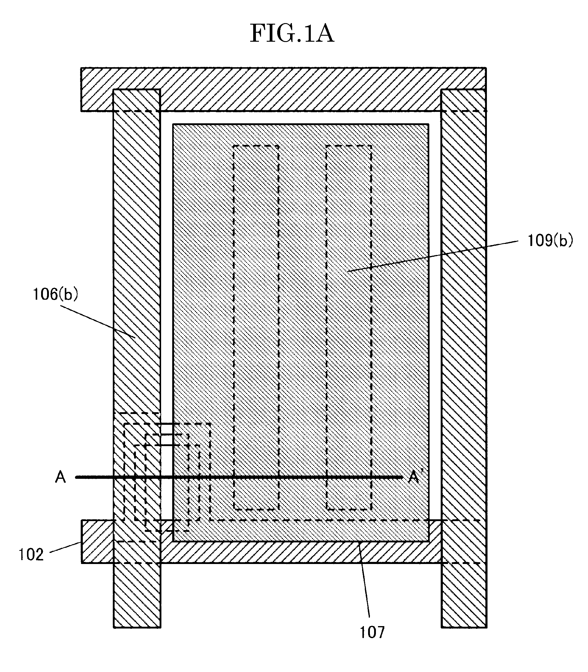
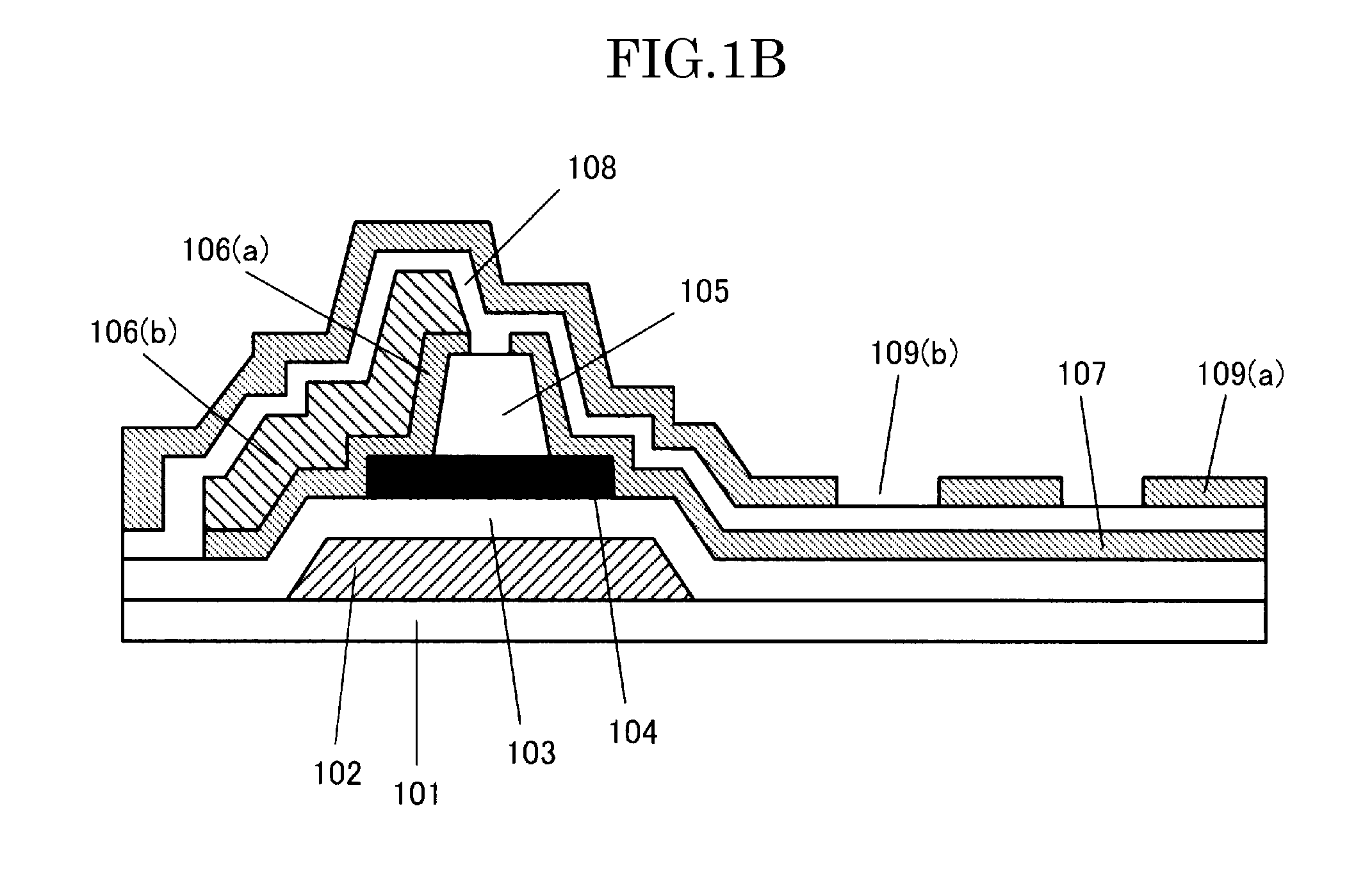
[0025]FIGS. 1A and 1B are diagrams for illustrating the display device according to the first embodiment of the present invention, where FIG. 1A is a plan diagram and FIG. 1B is a cross-sectional diagram along A-A′ in FIG. 1A.

[0026]As shown in FIG. 1B, the display device according to the present invention has: a gate electrode 102 formed on a transparent substrate 101; a gate insulating film 103 that covers the gate electrode 102; an oxide semiconductor 104 formed on top of the gate insulating film 103; a drain electrode 106 and a source electrode 107 formed at a distance from each other with a channel region in the oxide semiconductor 104 in between; an interlayer capacitor film 108 for covering the drain electrode 106 and the source electrode 107; a common electrode 109 formed on top of the interlayer capacitor film 108; and a pixel electrode 107 formed so as to face the common elect...


PUM


Abstract

The present invention provides a display device having: gate electrodes formed on a transparent substrate; a gate insulating film for covering the gate electrodes; an oxide semiconductor formed on the gate insulating film; drain electrodes and source electrodes formed at a distance from each other with channel regions of the oxide semiconductor in between; an interlayer capacitor film for covering the drain electrodes and source electrodes; common electrodes formed on top of the interlayer capacitor film; and pixel electrodes formed so as to face the common electrodes, and wherein an etching stopper layer for covering the channel regions is formed between the oxide semiconductor and the drain electrodes and source electrodes, the drain electrodes are a multilayer film where a transparent conductive film and a metal film are layered on top of each other, and the drain electrodes and source electrodes make direct contact with the oxide semiconductor.

Description

CROSS-REFERENCE TO RELATED APPLICATION[0001]The present application claims priority over Japanese Patent Application JP2012-134740 filed on Jun. 14, 2012, the contents of which are hereby incorporated into this application by reference.BACKGROUND OF THE INVENTION[0002](1) Field of the Invention[0003]The present invention relates to a display device and a manufacturing method for the same, and in particular, to a display device where an oxide semiconductor is used in the TFT circuit and a manufacturing method for the same.[0004](2) Description of the Related Art[0005]Various types of display devices, such as a liquid crystal module (liquid crystal display device) and an organic electroluminescent display device, are used as the display device for many portable type information apparatuses, such as a cellular phone, a portable information terminal (PDA), a digital camera and a multimedia player.[0006]An insulating substrate made of glass or a resin is used as a part of the display pan...

Claims


Application Information

Patent Timeline
Patent Type & Authority Applications(United States)
IPC IPC(8): H01L27/12
CPCH01L27/1244H01L27/1225H01L27/3244H01L27/1288H10K59/12H01L27/1255H01L29/45H01L29/78606H01L29/7869
Inventor MIYAKE, HIDEKAZUUEMURA, NORIHIRONODA, TAKESHISUZUMURA, ISAOKANEKO, TOSHIKI
Owner JAPAN DISPLAY INC
Why Eureka
Try Eureka