
Manufacturing method of circuit pattern

Inactive Publication Date: 2013-12-19
LEADING TECH COMM
View PDF9 Cites 2 Cited by
  • Summary
  • Abstract
  • Description
  • Claims
  • Application Information

AI Technical Summary

Benefits of technology

The present invention provides a method for making a three-dimensional circuit pattern on a substrate, which can improve the quality of the pattern and reduce associated costs. The method can use any substrate material and avoid color cast caused by conventional laser direct structuring. Additionally, the method can make the circuit pattern stick to the substrate efficiently, regardless of its shape.

Problems solved by technology

Therefore, the performance of the antenna may be affected.
The mentioned disadvantages related to the antenna or the circuit pattern made by the laser direct structuring process needs to be further improved.

Method used


Image

  • Manufacturing method of circuit pattern
  • Manufacturing method of circuit pattern
  • Manufacturing method of circuit pattern

Examples


Embodiment Construction

[0018]The aforementioned illustrations and following detailed descriptions are exemplary for the purpose of further explaining the scope of the instant disclosure. Other objectives and advantages related to the instant disclosure will be illustrated in the subsequent descriptions and appended drawings.

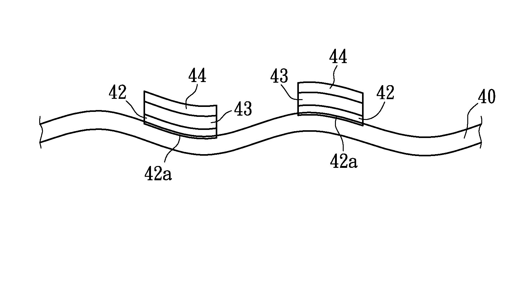
[0019]The instant disclosure provides a manufacturing method of circuit pattern. The method may be applied to making a three-dimensional or a curved circuit pattern on a substrate, such as an antenna structure. For ease of explanation, an antenna structure made by the manufacturing method is described in the following embodiment. However, this shouldn't be the limitation to the instant disclosure. In this embodiment, the substrate may be a casing of a smart phone, in which the casing of the smart phone usually is made by plastic or glass. However, the substrate material are not restricted thereto. In order to provide the circuit pattern with enough binding strength to the substrate, th...


PUM

PropertyMeasurementUnit
Thicknessaaaaaaaaaa
Thicknessaaaaaaaaaa
Diameteraaaaaaaaaa

Abstract

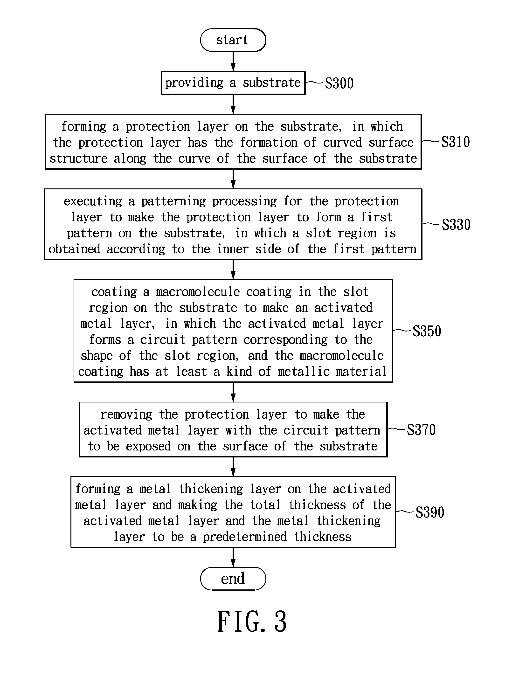
This instant disclosure provides a manufacturing method of circuit pattern. The method comprising, forming a substrate; forming a protection layer on the substrate for making the protection layer to be a curved surface along the surface of the substrate; executing a pattern processing for the protection layer to make the protection layer to form a first pattern on the substrate, wherein a slot region is obtained according to the inner side of the first pattern; coating a macromolecule coating to the slot region for forming an activated metal layer on the substrate, wherein the activated metal layer forms a circuit pattern respective to the slot region, the macromolecule coating includes at least a kind of metal material; removing the protection layer for exposing the activated metal layer with the circuit pattern. The manufacturing quality of the circuit pattern can be improved and the associated cost can be saved.

Description

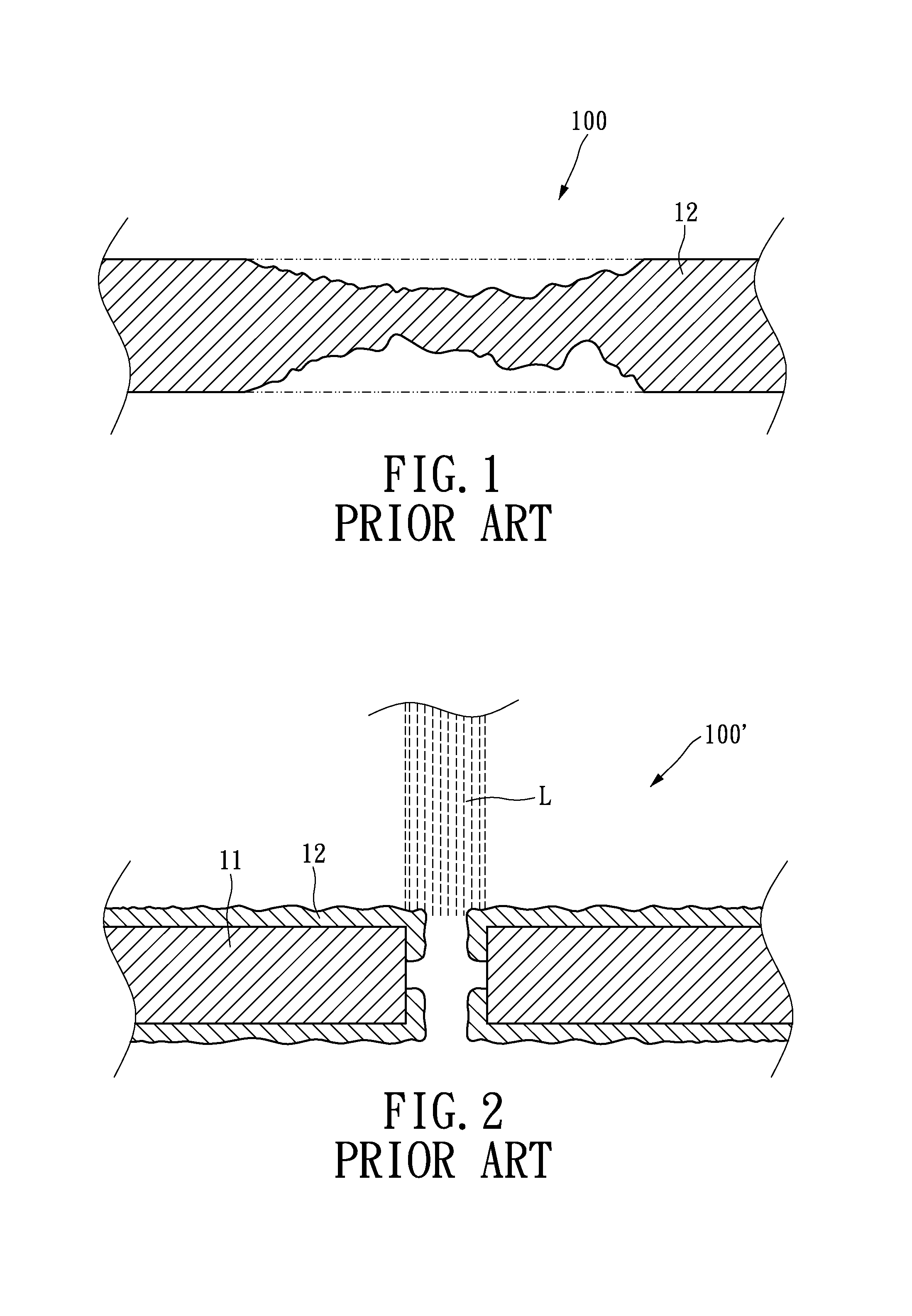
BACKGROUND OF THE INVENTION[0001]1. Field of the Invention[0002]The instant disclosure relates to a circuit pattern; in particular, to a manufacturing method of circuit pattern.[0003]2. Description of Related Art[0004]FIG. 1 and FIG. 2 show cross-sectional diagrams of a traditional antenna structure 100, 100′. As shown in FIG. 1, a laser direct structuring (LDS) process is applied to a substrate 11 to make a laser activated layer 12. The substrate 11 may be a casing of a mobile device (e.g. smart phone). The laser activated layer 12 may not accord to a predetermined line width (defined by the dashed lines) because some areas are not activated by the laser, thus a jump-plated phenomenon may be occurred. Therefore, the performance of the antenna may be affected. As shown in FIG. 2, when a laser beam L is applied to a via hole of the substrate 11 for making the laser activated layer 12, some area of the via hole wall may not be totally activated due to the diameter of the via hole, the...

Claims


Application Information

Patent Timeline
IPC IPC(8): H05K3/10H05K3/14C25D5/02H05K3/12
CPCC25D5/022C25D5/10C23C18/1651C23C18/1653C23C18/2066C23C18/206H05K3/1258H05K3/143H05K3/246H05K3/386H05K2203/0568H05K2203/107C25D5/627C25D5/56
Inventor HUANG, HSING YA
Owner LEADING TECH COMM
Learn More