

Thin Film Transistor Substrate Having Metal Oxide Semiconductor and Method for Manufacturing the Same
- Summary
- Abstract
- Description
- Claims
- Application Information
AI Technical Summary
Benefits of technology
Problems solved by technology
Method used
Image

Examples
Embodiment Construction
[0038]Referring to attached figures, preferred embodiments of the present disclosure will be described. Like reference numerals designate like elements throughout the detailed description. However, the present disclosure is not restricted by these embodiments but can be applied to various changes or modifications without changing the technical spirit. In the following embodiments, the names of the elements are selected for ease of explanation and may be different from actual names.
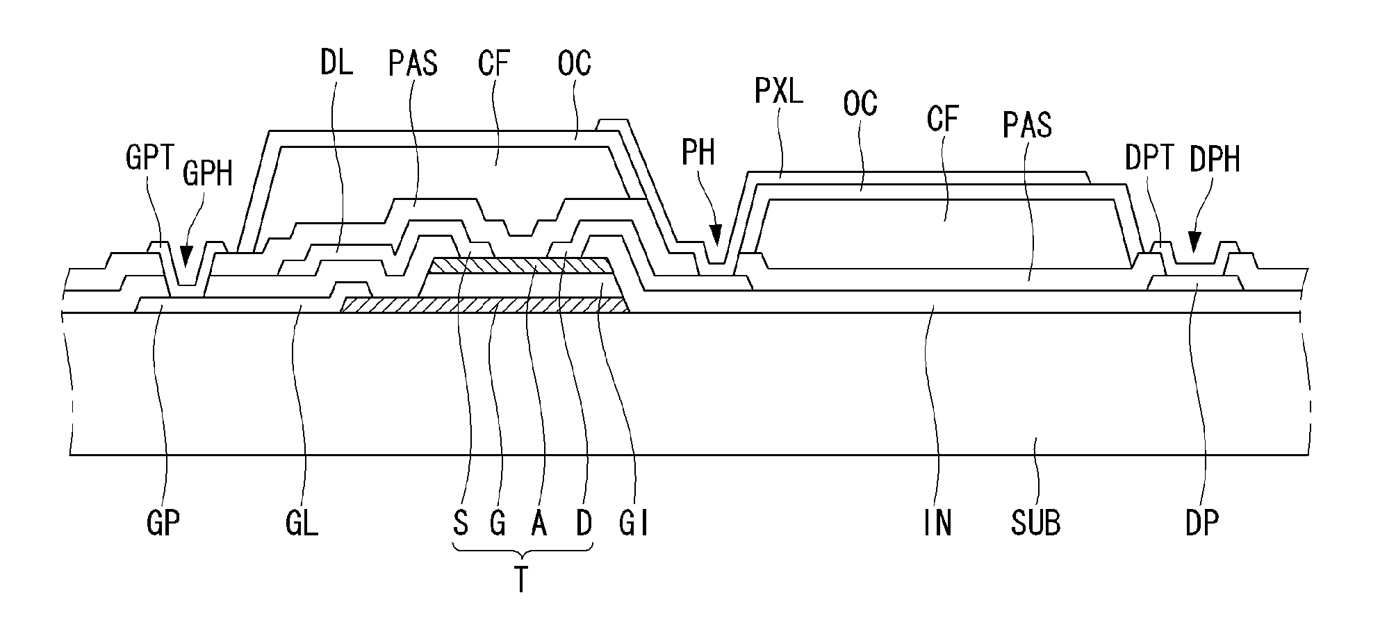
[0039]Referring to attached figures including FIG. 3 and FIGS. 4A to 4G, a method for manufacturing a thin film transistor substrate having a metal oxide semiconductor material will be described according to a first embodiment of the present disclosure. FIG. 3 is a plane view illustrating the structure of a thin film transistor substrate having a metal oxide semiconductor material according to the present disclosure. FIGS. 4A to 4G are cross-sectional views illustrating method steps for manufacturing a thi...
PUM
 Abstract
Description
Claims
Application Information