Semiconductor testing jig and semiconductor testing method performed by using the same

a technology of semiconductor testing and jig, which is applied in the direction of electronic circuit testing, measurement devices, instruments, etc., can solve the problems of degrading electrical characteristics, increasing vacuum, and partially damaged measurement targets

Active Publication Date: 2014-01-09
MITSUBISHI ELECTRIC CORP
View PDF56 Cites 2 Cited by
  • Summary
  • Abstract
  • Description
  • Claims
  • Application Information

AI Technical Summary

Problems solved by technology

However, increasing the tightness of contact for reducing the contact resistance, namely, increasing a degree of vacuum of the vacuum suction in turns degrades electrical characteristics.
If the foreign matter has a large size, a defect such as a crack is generated in a contact part with the measurement target and the vicinity of the contact part, so that the measurement target is damaged partially.
Meanwhile, even if the foreign matter has a relatively small size such as tens of μm or less that is hard to recognize visually, distortion due to pressure is still generated in the measurement target in the contact part with the measurement target and the vicinity of the contact part.
If a contact probe to make electrical contact for measuring electrical characteristics is brought into contact with the semiconductor wafer existing on the vacuum suction groove, the semiconductor wafer is also deformed due to contact pressure from the probe, thereby generating distortion.
However, providing a film or a sheet to all semiconductor substrates targeted for measurement leads to the problem of cost increase as it involves more manufacturing steps and an additional material.
So, the width cannot be reduced sufficiently enough to suppress deformation especially of a thin semiconductor wafer.
Additionally, reducing the width of the vacuum suction groove is additional work on an existing check stage, so that it involves interruption of a testing step and eventually, interruption of manufacturing steps.
This acts disadvantageously in terms of cost.

Method used


Image

  • Semiconductor testing jig and semiconductor testing method performed by using the same
  • Semiconductor testing jig and semiconductor testing method performed by using the same
  • Semiconductor testing jig and semiconductor testing method performed by using the same

Examples


Embodiment Construction

A. First Preferred Embodiment

A-1. Structure

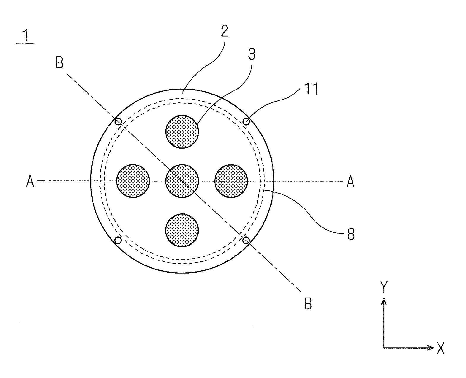
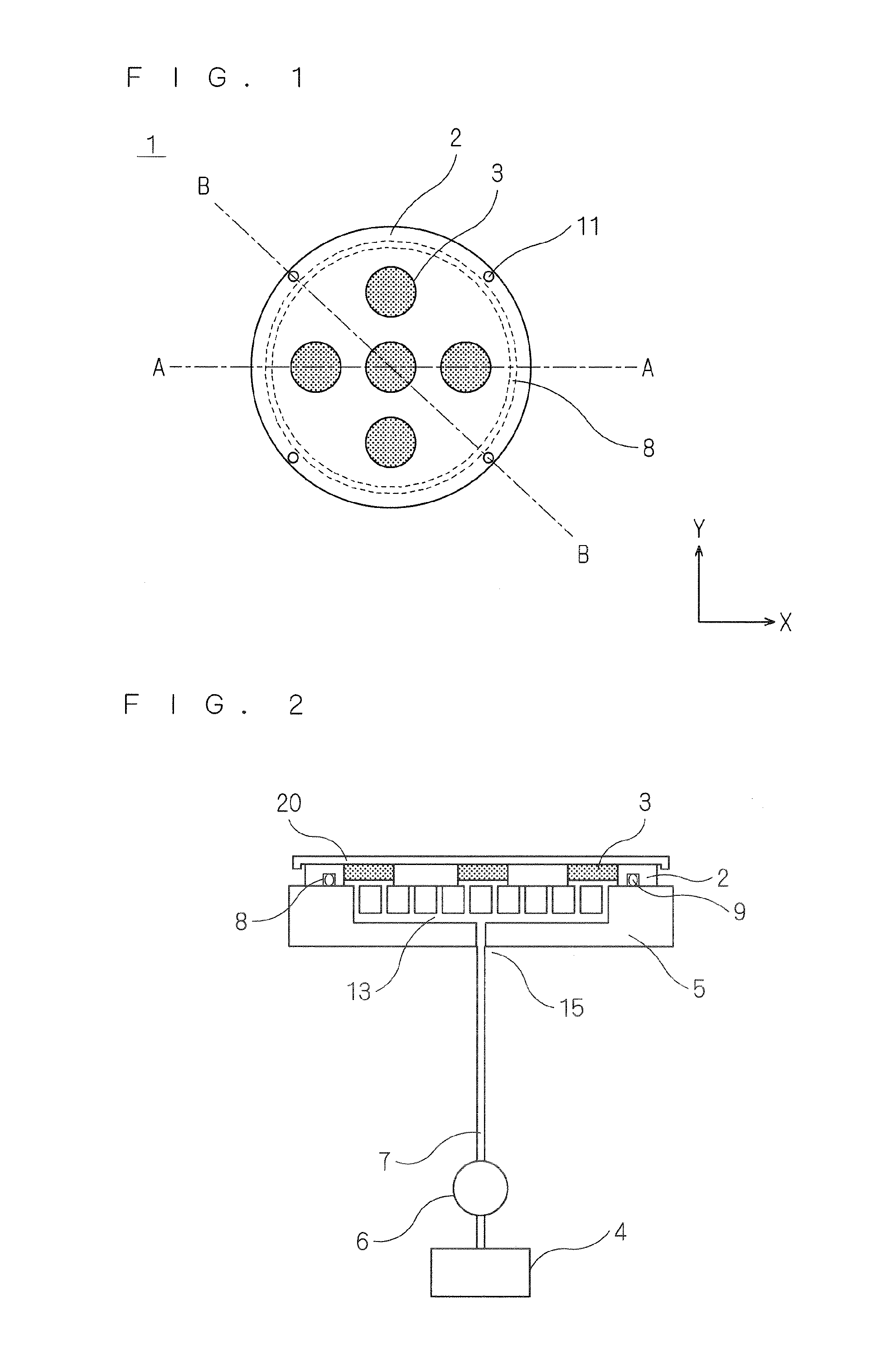
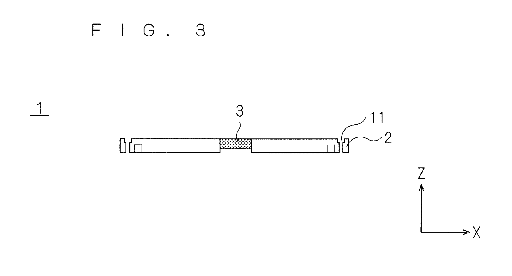
[0024]FIG. 1 is a top view of a semiconductor testing jig 1 of a first preferred embodiment. FIG. 2 is a sectional view taken along line A-A of FIG. 1 and showing a semiconductor testing device including the semiconductor testing jig 1. FIG. 3 is a sectional view taken along line B-B of FIG. 2 and showing the semiconductor testing jig 1.

[0025]As shown in FIG. 2, the semiconductor testing device of the first preferred embodiment includes a chuck stage 5 for vacuum suction, the semiconductor testing jig 1 placed on an installation surface of the chuck stage 5, a vacuum path 7 connected to a connection hole 15 of the chuck stage 5, a regulator 6 connected to the vacuum path 7, and a vacuum source 4.

[0026]The chuck stage 5 is an existing vacuum suction stage, and has a suction path 13 inside communicating with the connection hole 15. The suction path 13 communicates with an opening of the installation surface of the chuck stage 5.

[0027]The vacu...


PUM


Abstract

A semiconductor testing jig fixes a measurement target while it is held between a chuck stage and the measurement target. The semiconductor testing jig includes a base on which the measurement target is to be installed and which can be attached to the chuck stage. The base includes: a first main surface to become an installation surface for the measurement target; a second main surface opposite the first main surface and which is to contact the chuck stage; and a porous region containing a porous member. The porous region is provided selectively as seen in plan view, and penetrates through the base from the first main surface toward the second main surface.

Description

BACKGROUND OF THE INVENTION[0001]1. Field of the Invention[0002]The present invention relates to a semiconductor testing jig and a semiconductor testing method performed by using the same.[0003]2. Background Art[0004]According to technique generally employed for measurement of the electrical characteristics of a semiconductor wafer or a semiconductor chip, for example, a surface of a measurement target where the measurement target is to be placed on a chuck stage is fixed under suction to the chuck stage. If the measurement target is a vertical semiconductor that flows a current in the vertical direction, namely, in the out-of-plane direction of the measurement target, how tightly the measurement target and the chuck stage contact each other affects a contact resistance, and eventually, affects the electrical characteristics of the measurement target.[0005]However, increasing the tightness of contact for reducing the contact resistance, namely, increasing a degree of vacuum of the v...

Claims


Application Information

Patent Timeline
Patent Type & Authority Applications(United States)
IPC IPC(8): G01R31/28
CPCG01R31/2886G01R31/2887G01R31/2889
Inventor AKIYAMA, HAJIMEOKADA, AKIRAYAMASHITA, KINYA
Owner MITSUBISHI ELECTRIC CORP
Why Eureka
Try Eureka