Semiconductor device

a semiconductor device and a technology of semiconductor devices, applied in the direction of semiconductor devices, semiconductor/solid-state device details, electrical apparatus, etc., can solve the problems of increasing the lateral width of the package, the number of chips that can be arranged and the lateral width of each chip of a semiconductor device with a plurality of transistor chips arranged in a row is restricted by the lateral width, and the cost increase, so as to achieve the effect of improving the output without increasing the package size and deteriorating reliability

Active Publication Date: 2014-01-16
ROHM CO LTD
View PDF18 Cites 23 Cited by
  • Summary
  • Abstract
  • Description
  • Claims
  • Application Information

AI Technical Summary

Benefits of technology

[0012]The present invention makes it possible to improve output without increasing

Problems solved by technology

However, the number of chips that can be arranged and the lateral width of each chip of a semiconductor device with a plurality of transistor chips arranged in a row are restricted by the lateral width of its package.
Therefore, increasing the number of chips or increasing the lateral width of each chip results in an increase in the lateral width of the package, which leads to a cost increase.
Furthermore, when chips are arranged before or after each other, only ends of the chips can overlap each other to avoid wire contact, which prevents the package size from being reduced sufficiently.
However,

Method used


Image

  • Semiconductor device
  • Semiconductor device
  • Semiconductor device

Examples


first embodiment

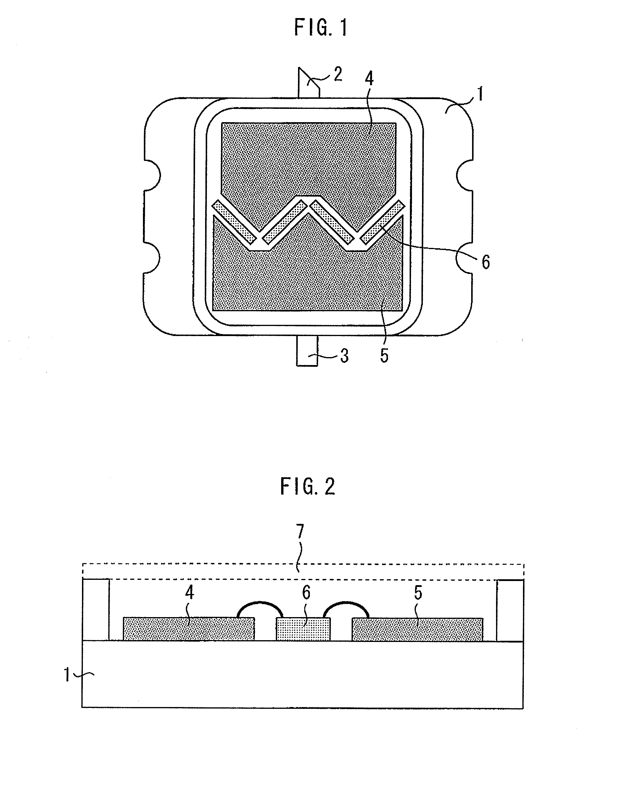
[0028]FIG. 1 is a plan view illustrating a semiconductor device according to the first embodiment of the present invention. FIG. 2 is a cross-sectional view along a line I-II in FIG. 1. An RF input terminal 2 for inputting an RF signal and an RF output terminal 3 for outputting an RF signal are provided on mutually opposite sides of a substantially rectangular package 1 in plan view. An input matching circuit 4 and an output matching circuit 5 are provided in the package 1, and are connected to the RF input terminal 2 and the RF output terminal 3 respectively. A plurality of transistor chips 6 are provided between the input matching circuit 4 and the output matching circuit 5 in the package 1. The top surface of the package 1 is covered with a lid 7.

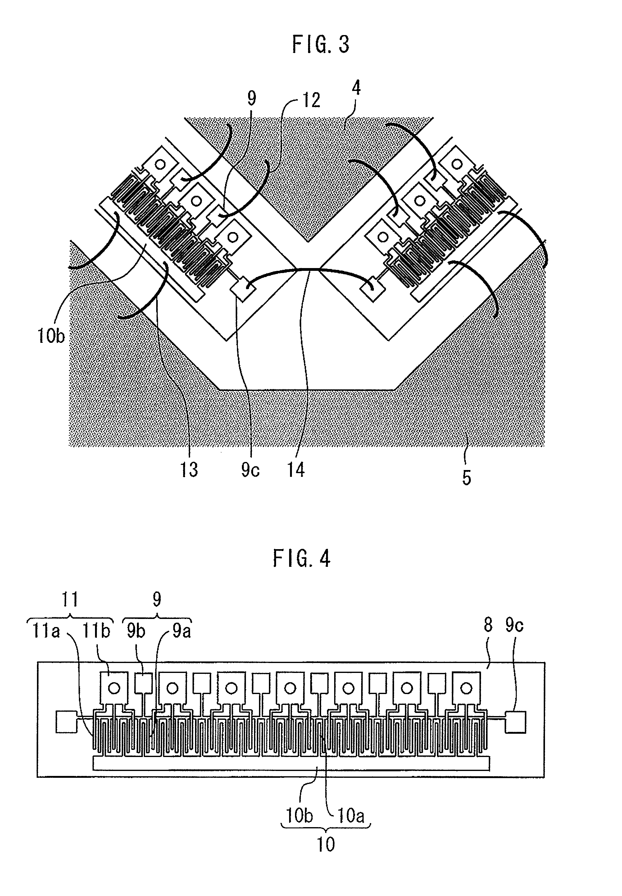
[0029]FIG. 3 is an enlarged plan view of the transistor chip in FIG. 1. FIG. 4 is a plan view illustrating the transistor chip according to the first embodiment of the present invention. Each transistor chip 6 includes a rectangular semi...

second embodiment

[0038]FIG. 9 is a plan view illustrating a semiconductor device according to the second embodiment of the present invention. FIG. 10 is an enlarged plan view of the transistor chips in FIG. 9. The shape of the transistor chip 6 is not a normal rectangle but a parallelogram. The short sides of the semiconductor substrates 8 of the plurality of transistor chips 6 are parallel with respect to the input / output direction.

[0039]If the rectangular transistor chip 6 is provided with chip coupling gate pads 9c at the ends of the chip, the area of the region where the gate fingers 9a are provided decreases. In contrast, the present embodiment allows the chip coupling gate pads 9c to be provided in gaps between the chips, and can thereby expand the area of the region where the gate fingers 9a are provided. Therefore, the output can be further improved without increasing the package size.

[0040]The semiconductor substrate 8 of the transistor chip 6 is made of SiC and a GaN-based HEMT is provided...

third embodiment

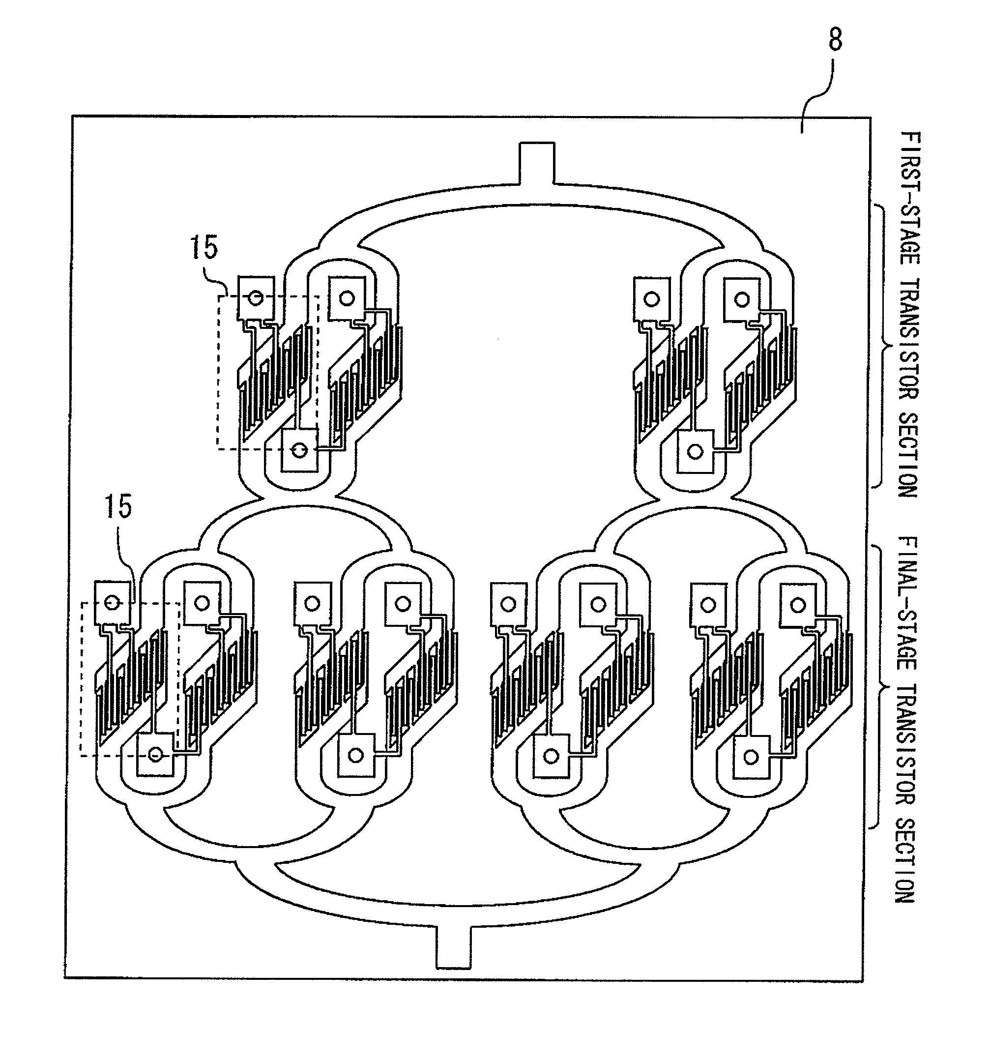
[0042]FIG. 11 is a plan view illustrating a semiconductor device according to the third embodiment of the present invention. FIG. 12 is a partially enlarged plan view of FIG. 11. This semiconductor device is an MMIC including a first-stage transistor section that amplifies an input signal and a final-stage transistor section that further amplifies the output signal

[0043]A plurality of transistor cells 15 are provided on a semiconductor substrate 8. In each transistor cell 15, a plurality of gate fingers 9a are arranged in a diagonal rectilinear form. On the boundary between adjacent transistor cells 15, the gate fingers 9a at the ends of the transistor cells 15 are shifted from each other. This prevents heat from being concentrated on the cell boundary and prevents deterioration of characteristics and reliability caused by a temperature rise. According to a simple thermal resistance calculation result using a simulation, the present embodiment can reduce the thermal resistance value...


PUM


Abstract

A semiconductor device includes: a package; an input matching circuit and an output matching circuit in the package; and transistor chips between the input matching circuit and the output matching circuit in the package. Each transistor chip includes a semiconductor substrate having long sides and short sides that are shorter than the long sides, and a gate electrode, a drain electrode and a source electrode on the semiconductor substrate. The gate electrode has gate fingers arranged along the long sides of the semiconductor substrate and a gate pad commonly connected to the gate fingers and connected to the input matching circuit via a first wire. The drain electrode is connected to the output matching circuit via a second wire. The long sides of the semiconductor substrates of the transistor chips are oblique with respect to an input/output direction extending from the input matching circuit to the output matching circuit.

Description

BACKGROUND OF THE INVENTION[0001]1. Field of the Invention[0002]The present invention relates to a semiconductor device capable of improving output without increasing its package size and causing deterioration of its characteristics and reliability.[0003]2. Background Art[0004]High output semiconductor devices are required to amplify an inputted RF signal and output power of several W to several hundreds of W. The gate width of transistors used for such semiconductor devices needs to be several mm to several hundreds of mm. Transistors having such a large gate width need to be fitted into a package of merely several mm to several tens of mm in size. Thus, one to four or so transistor chips with an array of several tens to a hundred or so of gate fingers having a gate width (gate finger length) of several tens of μm to several hundreds of mm are arranged in a package.[0005]Conventional semiconductor devices have a plurality of transistor chips arranged in a row so that their respecti...

Claims


Application Information

Patent Timeline
IPC IPC(8): H01L27/08H01L29/16
CPCH01L27/08H01L29/1608H01L2224/48091H01L2224/48137H01L27/0207H01L2224/45144H01L2924/30107H01L29/267H01L29/41758H01L29/42316H01L29/7786H01L29/0657H01L29/2003H01L24/06H01L24/45H01L24/48H01L24/49H01L2224/0612H01L23/4824H01L23/66H01L2223/6611H01L2223/6644H01L2223/6655H01L2224/49H01L2224/05554H01L2924/16195H01L2924/00014H01L2924/00
Inventor KUNII, TETSUOTSUJI, SEIICHIKOYANAGI, MOTOYOSHI
Owner ROHM CO LTD
Why Eureka
Try Eureka