
Method of replacing silicon with metal in integrated circuit chip fabrication

a technology of integrated circuits and metal contacts, which is applied in the direction of semiconductor devices, electrical equipment, transistors, etc., can solve the problems of increasing chip power consumption, increasing cooling and packaging costs, and typical fets being much more complex than switches, so as to reduce the pinch off of replacement metal contacts

Inactive Publication Date: 2014-01-16
GLOBALFOUNDRIES INC
View PDF14 Cites 2 Cited by
  • Summary
  • Abstract
  • Description
  • Claims
  • Application Information

AI Technical Summary

Benefits of technology

The patent aims to address three technical problems in ICs: reducing short channel effects without affecting performance, improving replacement metal gate FET chip reliability and quality, and improving replacement metal contact reliability and quality. Additionally, it aims to reduce pinch off in replacement metal contacts.

Problems solved by technology

Thus, notwithstanding the decrease of chip supply voltage, chip power consumption has increased as well.
At both chip level and system level, cooling and packaging costs have escalated as a natural result of this increase in chip power.
However, since improving performance means running circuits faster (with higher switching speeds), reducing chip power consumption is at odds with improving performance.
In practice, however, typical FETs are much more complex than switches.
Especially for complex chips and arrays with a large number of devices, short channel effects can be overwhelming.
When multiplied by the millions and even billions of devices on a state of the art IC, even 100 picoAmps (100 pA) of leakage in each of a million circuits, for example, results in chip leakage on the order of 100 milliAmps (100 mA).
Unfortunately, however, polysilicon cannot be used with high-k dielectrics.
This strain causes these narrow aspect ratio trenches to buckle and partially collapse, such that frequently the top of some trenches close (pinch off).
Even in those metal gates that form with voids, the voids can introduce resistance or act as a dielectric above the high-k dielectric, randomly altering device characteristics unintentionally.
Missing contacts can cause a circuit and chip failure, i.e., yield loss.
This random resistance can cause erratic failures that are difficult to identify and may not manifest until a chip is in place in the field.
These missing contacts and contact voids raise manufacturing costs and degrade chip quality, making it difficult to reliably make consistent structures.
Consequently, trench aspect ratio has been a limit both on reducing RMG device length and on increasing contact density.

Method used


Image

  • Method of replacing silicon with metal in integrated circuit chip fabrication
  • Method of replacing silicon with metal in integrated circuit chip fabrication
  • Method of replacing silicon with metal in integrated circuit chip fabrication

Examples


Embodiment Construction

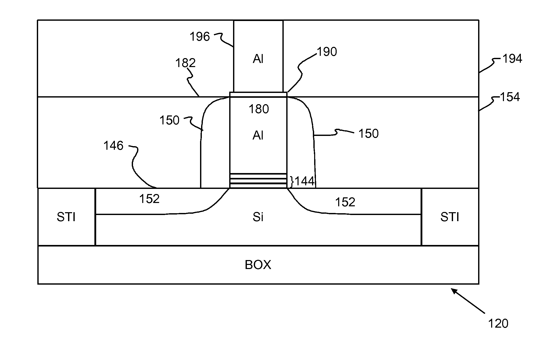
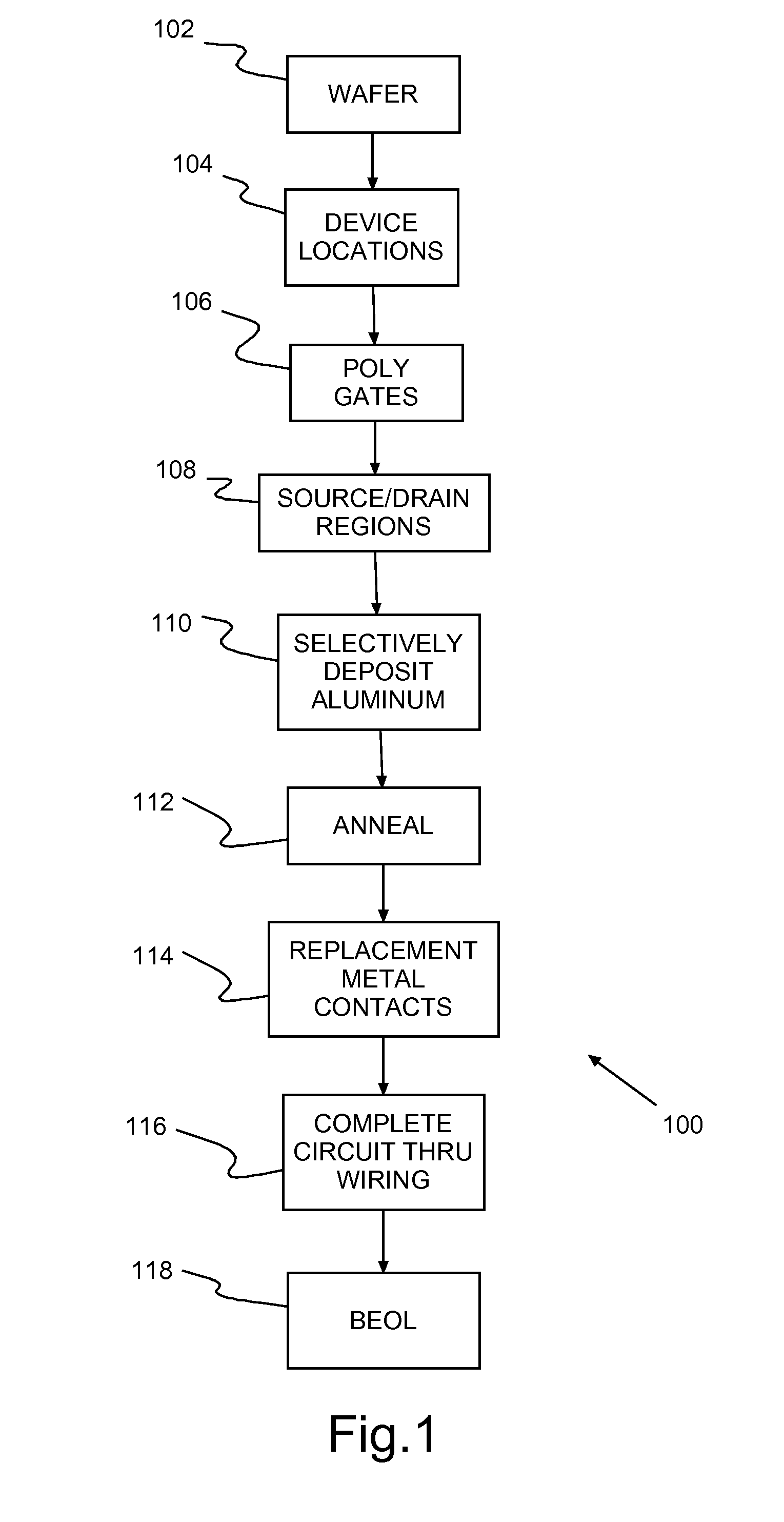
[0036]Turning now to the drawings and, more particularly, FIG. 1 shows an example of a method 100 of forming semiconductor devices, Replacement Metal Gate (RMG) gate Field Effect Transistors (FETs) or RMGFETs, as well as optionally or alternately form Replacement Metal Contacts (RMCs), according to a preferred embodiment of the present invention. Although described with reference to silicon on insulator (SOI) technology, and more particularly CMOS, the present invention has application to any suitable replacement metal technology. Further, the preferred method 100 has application to forming ICs with only RMGFETs or RMC or both.

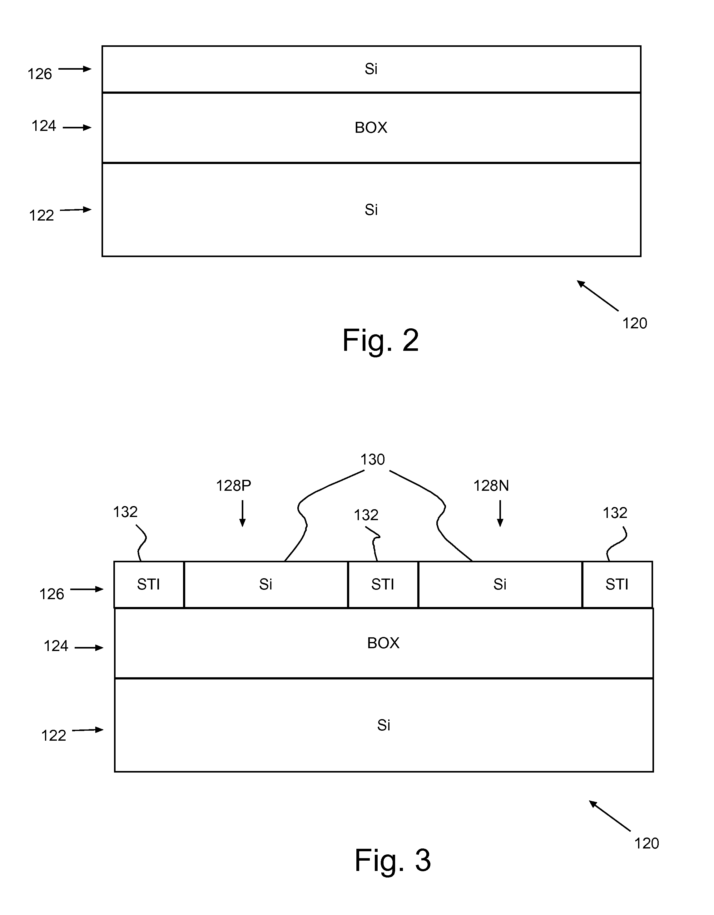
[0037]IC fabrication begins with a preparing 102 a semiconductor wafer, e.g., an SOI wafer. Device locations are defined 104 on the silicon surface layer of the multilayered SOI wafer. Semiconductor, preferably silicon, gates are formed 106 in the device locations. Metal, preferably aluminum (Al), is deposited 110 on the silicon gates. The wafer is annealed 11...


PUM


Abstract

A method of replacing semiconductor material with metal, Replacement Metal Gate Field Effect Transistors (RMG FETs) and Contacts (RMCs), and Integrated Circuit (IC) chips including the FETs and / or RMCs. A patterned semiconductor layer, e.g., silicon, is formed on a dielectric layer, e.g., a layered gate dielectric. A field dielectric layer fills between shapes in the patterned semiconductor layer. Metal is deposited on the shapes. The wafer is annealed to replace semiconductor in each shape with metal to form metal FET gates or contacts.

Description

CROSS REFERENCE TO RELATED APPLICATION[0001]The present invention is a divisional of U.S. application Ser. No. 13 / 310,796 (Attorney Docket No. YOR920110478US1) “METHOD OF REPLACING SILICON WITH METAL IN INTEGRATED CIRCUIT CHIP FABRICATION” to Kevin K. Chan et al., filed Dec. 5, 2011, assigned to the assignee of the present invention and incorporated herein by reference.BACKGROUND OF THE INVENTION[0002]1. Field of the Invention[0003]The present invention generally relates to Integrated Circuit (IC) manufacture and more particularly to reducing costs in semiconductor chip manufacture of integrated circuits with Field Effect Transistors (FETs) with metal gates and / or metal contacts.[0004]2. Background Description[0005]A primary goal in integrated circuit (IC) chip manufacturing is increasing chip density and performance, i.e., placing more function that operates at higher speeds. To achieve that goal, semiconductor technology and chip manufacturing advances have steadily decreased chip...

Claims


Application Information

Patent Timeline
Patent Type & Authority Applications(United States)
IPC IPC(8): H01L27/088
CPCH01L27/088H01L21/823437H01L21/823481H01L21/84H01L27/1203H01L21/76886H01L21/76879H01L29/4908H01L29/66772H01L21/76283
Inventor CHAN, KEVIN K.D'EMIC, CHRISTOPHERKIM, YOUNG-HEEPARK, DAE-GYUYAU, JENG-BANG
Owner GLOBALFOUNDRIES INC
Learn More