Lens-equipped optical semiconductor device and method for manufacturing the same

a technology of optical semiconductor and resin lens, which is applied in the direction of semiconductor/solid-state device manufacturing, semiconductor devices, electrical devices, etc., can solve the problems of uneven positioning of transparent resin encapsulating bodies, inability to obtain light distribution characteristics as designed, and inability to achieve light distribution uniformity. , to achieve the effect of high accuracy

Active Publication Date: 2014-01-30
ASAHI RUBBER
View PDF3 Cites 28 Cited by
  • Summary
  • Abstract
  • Description
  • Claims
  • Application Information

AI Technical Summary

Benefits of technology

[0017]According to the present invention, any offset of the position of the transparent resin encapsulating body with respect to the position of the optical semiconductor element can be corrected

Problems solved by technology

However, the LED device production method including the overmolding process as described above has a problem in that the arrangement position of the transparent resin encapsulating body is offset with respect to the position of the center of the LED elements.
This has posed the problem that the light distribution characteristics as designed cannot be obtained when the center of the LED el

Method used


Image

  • Lens-equipped optical semiconductor device and method for manufacturing the same
  • Lens-equipped optical semiconductor device and method for manufacturing the same
  • Lens-equipped optical semiconductor device and method for manufacturing the same

Examples


example 1

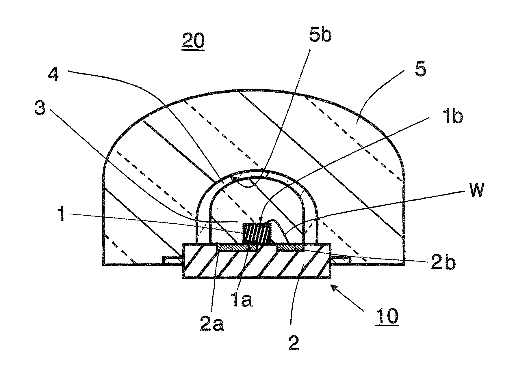
[0096]As an uncured silicone elastomer A1, 0E-6636 (manufactured by Dow Corning Toray Co., Ltd.; JIS A hardness after curing of 90; refractive index of 1.54) was poured into a mold including a cavity, and heat-cured at 150° C., thus yielding a silicone lens X1, which is a batwing lens having a shape such as shown in FIG. 13. The silicone lens X1 includes a lens portion of a shape having a major axis of 10 mm and a height of 5 mm and including two hemispherical elevations, and the lens portion includes a recessed portion having a diameter of 5.4 mm, a height of 2.6 mm, and a capacity 0.04 cm3 at the center of the rear face. Also, a slight degree of tackiness without adhesiveness was perceived on the surface of the silicone lens X1.

[0097]Then, as an uncured silicone elastomer B1, 0.02 cm3 of TSE3221S (manufactured by Momentive Performance Materials Japan LLC.; JIS A hardness after curing of 30; refractive index of 1.41) was filled into the recessed portion of the silicone lens X1 usin...

example 2

[0104]A lens-equipped LED device B was obtained in the same manner as in Example 1 except that an overmolded LED device in which the center of the LED element and the center of the encapsulating body were offset by 100 μm was used as the overmolded LED device. FIG. 16 is a graph showing the light distribution characteristics of the above-described overmolded LED device, and FIG. 17 is a graph showing the light distribution characteristics of the obtained lens-equipped LED device B. As can be seen in the graph in FIG. 16, an asymmetrical peak indicating non-uniform emission at orthogonal coordinates was shown when the center of the LED element and the center of the encapsulating body were offset by 100 μm. However, as shown in the graph in FIG. 17, the lens-equipped LED device B including the silicone lens X1 showed batwing-like light distribution characteristics having symmetrical peaks indicating uniform emission at orthogonal coordinates, as in the case of the lens-equipped LED de...

example 3

[0105]A silicone lens X2 was formed in the same manner as in Example 1 except that an uncured hard silicone resin A2, SR7010 (manufactured by Dow Corning Toray Co., Ltd.; JIS D hardness after curing of 70; refractive index of 1.53) was used in place of the uncured silicone elastomer Al. Almost no tackiness was observed on the surface of the silicone lens X2. A lens-equipped LED device C was obtained in the same manner as in Example 1 except that the silicone lens X2 was used in place of the silicone lens X1. As a result of examining the light distribution characteristics of the obtained lens-equipped LED device C, the LED device C had batwing-like light distribution characteristics having symmetrical peaks indicating uniform emission at orthogonal coordinates, as in Example 1. Further, only a few voids were found as a result of examining the interface between the transparent resin layer and the transparent resin encapsulating body, and the bonding interface between the transparent r...


PUM


Abstract

A lens-equipped optical semiconductor device including: an optical semiconductor device including at least one optical semiconductor element mounted on a substrate and a transparent resin encapsulating body that encapsulates the optical semiconductor element; a resin lens having a recessed portion for housing the transparent resin encapsulating body; and a transparent resin layer filled into a space among the substrate, the recessed portion, and the transparent resin encapsulating body, wherein the recessed portion has a capacity that is at least 1.1 times a total volume of the optical semiconductor element and the transparent resin encapsulating body.

Description

BACKGROUND[0001]1. Field of the Invention. The present invention relates to an optical semiconductor device including a resin lens. More particularly, the invention relates to a technique for improving the light distribution accuracy of an optical semiconductor device including a resin lens.[0002]2. Description of the Related Art. The applications of LED devices using light-emitting diodes (LEDs) have been expanding in recent years. Specifically, such LED devices are used, for example, for general indoor light fittings, spotlights such as courtesy lights, backlights of flat-screen televisions and information terminal devices, car taillights, street lights, traffic lights, and so forth.[0003]A general LED device includes a transparent resin encapsulating body for protecting a LED element (also referred to as a LED chip) mounted on a submount substrate. As shown in FIG. 19, a hemispherically molded transparent resin encapsulating body 3 for encapsulating an LED element 1 mounted on a ...

Claims


Application Information

Patent Timeline
IPC IPC(8): H01L33/52
CPCH01L33/52H01L33/58H01L2933/005H01L24/97H01L2224/48091H01L2224/45144H01L2924/12041H01L2924/15787H01L2924/181H01L2924/12042H01L2924/00014H01L2924/00H01L2924/0002
Inventor TASAKI, MASUTSUGUICHIKAWA, AKIRASATO, HIDEAKIENDO, SATOSHIMOTOYANAGI, TAKAYUKIOKABE, YOSHIHIROORIKASA, YOICHIAZUMA, MASARU
Owner ASAHI RUBBER
Why Eureka
Try Eureka