Wireless identification tag, electronic product PCB having same, and system for managing electronic products

Active Publication Date: 2014-02-06
NETHOM
View PDF2 Cites 45 Cited by
  • Summary
  • Abstract
  • Description
  • Claims
  • Application Information

AI Technical Summary

Benefits of technology

[0038]According to the present invention, follow-up management including assembly process management over electronic product PCBs becomes easy and rapid.
[0039]In particular, since the RFID tag according to the present invention

Problems solved by technology

Describing the foregoing management method using barcode labels, there are restrictions in that the miniaturization of labels is limited, and that labels must be attached to positions where they can be exposed at any time to a scanner.
In addition, scanning and processing time that reaches up to several tens of seconds can cause a time delay in the entire assembly process.
If an electronic product PCB is small, for example, is slightly larger than or similar

Method used


Image

  • Wireless identification tag, electronic product PCB having same, and system for managing electronic products
  • Wireless identification tag, electronic product PCB having same, and system for managing electronic products
  • Wireless identification tag, electronic product PCB having same, and system for managing electronic products

Examples


first embodiment

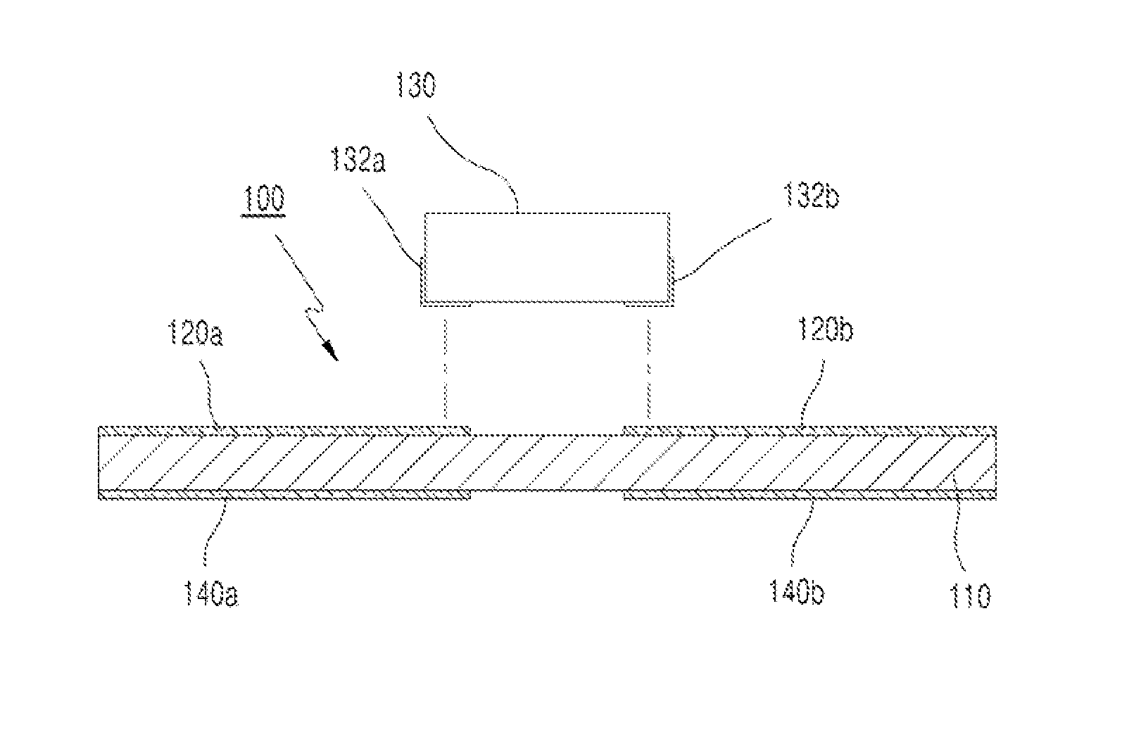
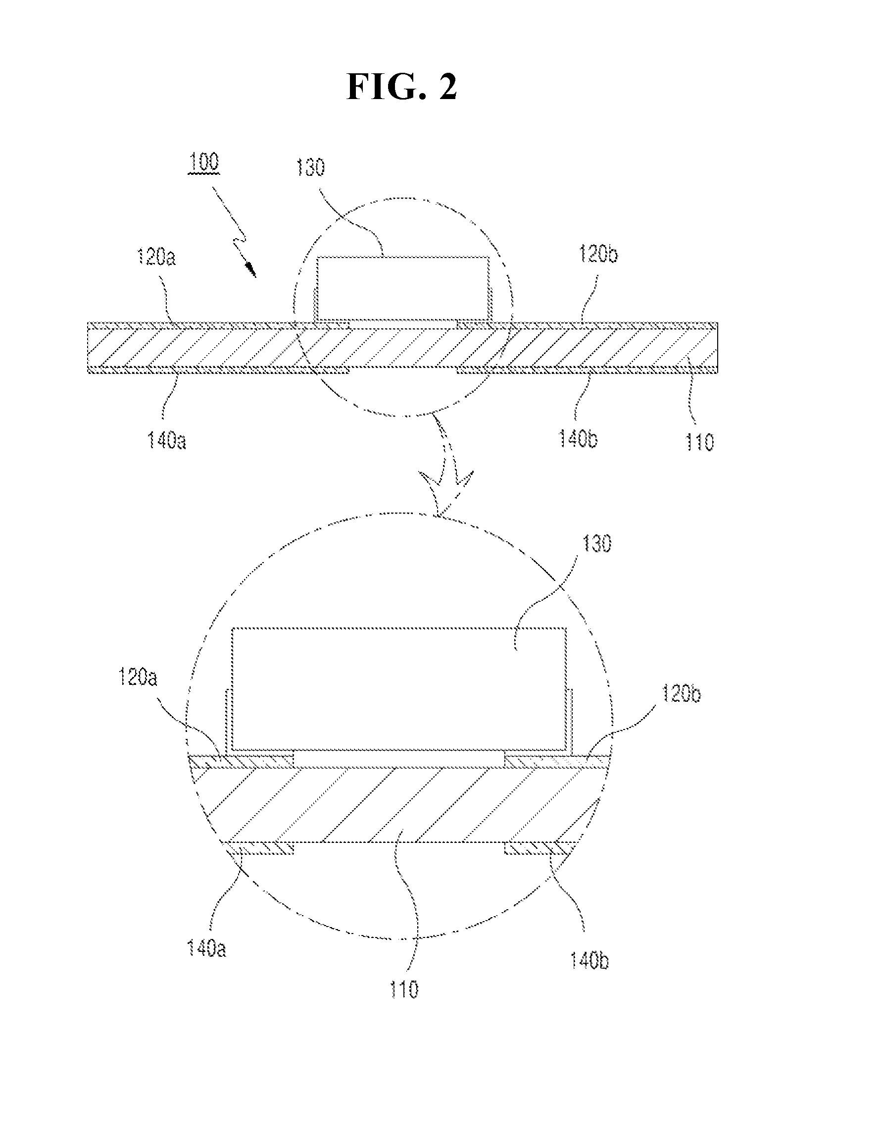
[0051]Referring to FIG. 1 and FIG. 2 in the accompanying drawings, a wireless identification or RFID tag 100 according to the invention includes an insulating means 110, upper terminals 120a and 120b, a tag chip 130 and lower terminals 140a and 140b.

[0052]The insulating means 110 may be understood as a dielectric medium that has a preset level of permittivity (∈). The insulating means 110 can be made of a variety of materials, such as plastic, paper, or ceramic, with the permittivity being variable depending on the material and thickness.

[0053]In FIG. 3A is a view showing the upper surface (upper portion) of the RFID tag 100 shown in FIG. 1, and FIG. 3B is a view showing the lower surface (bottom) of the RFID tag 100 shown in FIG. 1. A pair of the upper terminals 120a and 120b is provided on the upper surface of the insulating means 110, spaced apart from each other. The tag chip 130 is connected to the upper terminals 120a and 120b. The tag chip 130 has a pair of terminals 132a an...

second embodiment

[0058]A description will be given below of the RFID tag according to the invention.

[0059]The RFID tag according to the second embodiment is designated with reference numeral “200” in FIG. 6 to FIG. 8. The RFID tag 200 indicates a surface-mount device (SMD) produced by standardizing the RFID tag 100 according to the first embodiment through surface mounting. For reference, of course, the RFID tag 100 according to the first embodiment also corresponds to a surface-mounting type.

[0060]Specifically, referring to FIG. 6, the RFID tag 200 includes a tag chip 210 which has defined therein inner terminals 212a and 212b, an insulating body 220 which contains the tag chip 210 therein, and a pair of outer terminals 230a and 230b which are provided on the outer portions of the insulating body so as to face the inner terminals 212a and 212b.

[0061]Although the insulating body 220 can be made of the materials of the insulating body 110 according to the first embodiment, the present invention is n...

third embodiment

[0066]FIG. 9 and FIG. 10 are views illustrating an electronic product PCB 10 according to the invention.

[0067]Referring to the figures, a first isolating pad 16a and a second isolating pad 16b are provided on the upper surface of the electronic product PCB 10 such that the first and second isolating pads 16a and 16b are spaced apart from each other at a preset distance. Herein, the term “isolating” indicates the state in which each of the pads 16a and 16b is not physically connected to any pattern (the power pattern, ground pattern or signal pattern) formed on the electronic product PCB. A tag chip 18 is connected to the isolating pads 16a and 16b.

[0068]First and second lower pads 12a and 14b are provided on the lower surface of the electronic product PCB 10. The first lower pad 12a extends from the first pattern 12 so as to face the first isolating pad 16a, and the second lower pad 14b extends from the second pattern 14 so as to face the second isolating pad 16b. Preferably, the f...


PUM


Abstract

A wireless identification (RFID) tag, an electronic product PCB having same, and an electronic product management system using the RFID tag. The RFID tag includes an insulating means, a pair of upper terminals provided on the upper surface of the insulating means, a tag chip connected to the upper terminals, and a pair of lower terminals provided on the lower surface of the insulating means so as to face the upper terminals. The lower terminals are connected to first and second patterns of an electronic product PCB. When a radio wave radiated from a reader-writer is received in the first and second patterns, reactive coupling through an electric field is created between the upper and lower terminals, which are then electrically connected to the upper terminals. Since the pattern already formed in the PCB is used as an antenna, there is no need to form a dedicated antenna pattern.

Description

TECHNICAL FIELD[0001]The present invention relates, in general, to a wireless identification or radio frequency identification (RFID) tag, more particularly, to an RFID tag that is used for follow-up management including management over an assembly process of a variety of electronic products, and still more particularly, to an RFID tag that does not need a separate antenna.BACKGROUND ART[0002]Electronic products, such as TVs, mobile phones, computers or portable music players, include at least one printed circuit board (PCB). Such PCBs are subjected to the processes of assembling and inspecting parts, such as electronic components, in a production line.[0003]Barcode labels were used as an approach to manage the process of assembling electronic product PCBs (including the inspection process) in the related art. For instance, this method manages the entire processes including the assembly process by identifying barcodes printed on a barcode label using a scanner and updating the ident...

Claims


Application Information

Patent Timeline
IPC IPC(8): G06K19/07G06K19/14
CPCG06K19/14G06K19/0723G06K19/07758G06K19/07
Inventor LEE, GUN-HONG
Owner NETHOM
Why Eureka
Try Eureka