Copper Post Solder Bumps on Substrates

a copper post and substrate technology, applied in the field of electrical interconnections, can solve the problems of difficult cleaning of flux residue, and achieve the effects of reducing the stress on the resultant structure, eliminating or minimizing void formation, and easy cleaning of flux residu

Inactive Publication Date: 2014-02-27
INT BUSINESS MASCH CORP
View PDF2 Cites 11 Cited by
  • Summary
  • Abstract
  • Description
  • Claims
  • Application Information

AI Technical Summary

Benefits of technology

[0036]3. forming high volume IMS solder bumps on the distal ends of the Cu posts on the substrate to reduce the size and volume of the solder bumps on the wafer or eliminate the bumps on the wafer.
[0037]3. fabrication of selectively different bump structures by combining solder only and solder with a Cu post on one substrate to inter alia decrease the stress in Cu / ultra low k layers.
[0040]6. employing the openings in the mask as reservoirs for receiving molten solder wherein the reservoir and the posts sealingly engage one another toward the proximal ends of the post in a manner to substantially minimize or eliminate the leakage of molten solder from the reservoir. In one embodiment we achieve this function by employing posts that taper from the proximal ends toward the distal ends in a narrowing fashion. This can also be achieved by employing reservoirs that taper from the point of solder injection toward the other end of the reservoir in a narrowing fashion, Also, both tapered posts and tapered reservoirs can be employed. An advantage in using tapered posts comprises easier insertion and / or alignment of the posts in the reservoir.
[0046]The present invention, however, overcomes the difficulties of low stand off heights by placing injection molded solder on Cu posts to produce high bumps on substrates and helps to maintain high stand off heights after flip chip assembly which in turn provides the benefit of not only further decreasing the stress on the resultant structure, but also providing a structure where it is easy to clean the flux residue, underfill flow is easy thereby eliminating or minimizing void formation compared to prior processes, and minimizing or eliminating high stresses from the CTE mismatch between the chip or wafer and the organic substrate.

Problems solved by technology

The disadvantages of low stand off heights are:(1) it is difficult to clean flux residue;(2) underfill flow is not easy, so voids are formed; and(3) high stress from the CTE (Coefficient of thermal expansion) mismatch between the chip or wafer and the organic substrate.

Method used


Image

  • Copper Post Solder Bumps on Substrates
  • Copper Post Solder Bumps on Substrates
  • Copper Post Solder Bumps on Substrates

Examples


Embodiment Construction

[0064]To achieve these and other advantages, and in accordance with the purpose of this invention as embodied and broadly described herein, the following detailed embodiments comprise disclosed examples that can be embodied in various forms.

[0065]The specific processes, compounds, compositions, and structural details set out herein not only comprise a basis for the claims and a basis for teaching one skilled in the art to employ the present invention in any novel and useful way, but also provide a description of how to make and use this invention.

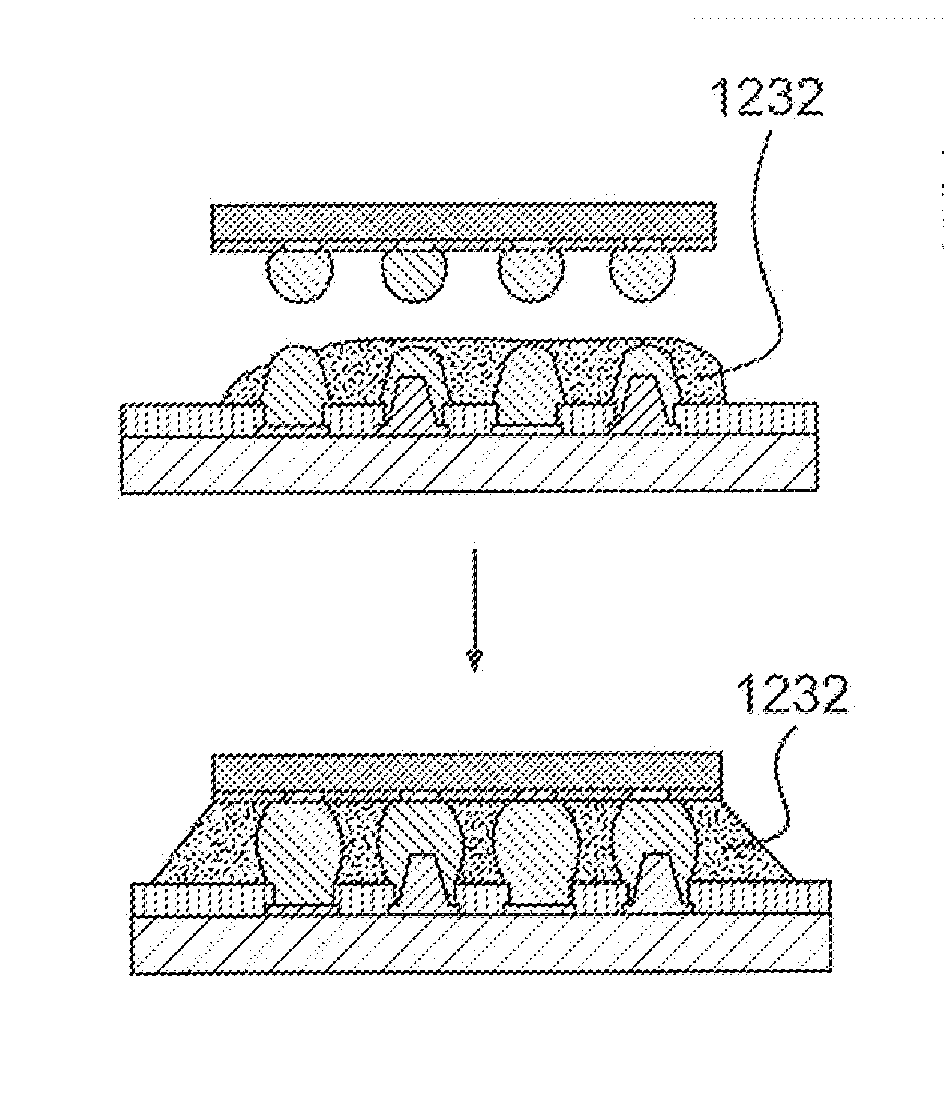
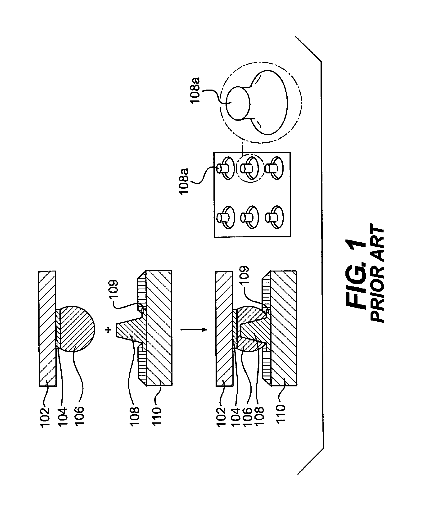
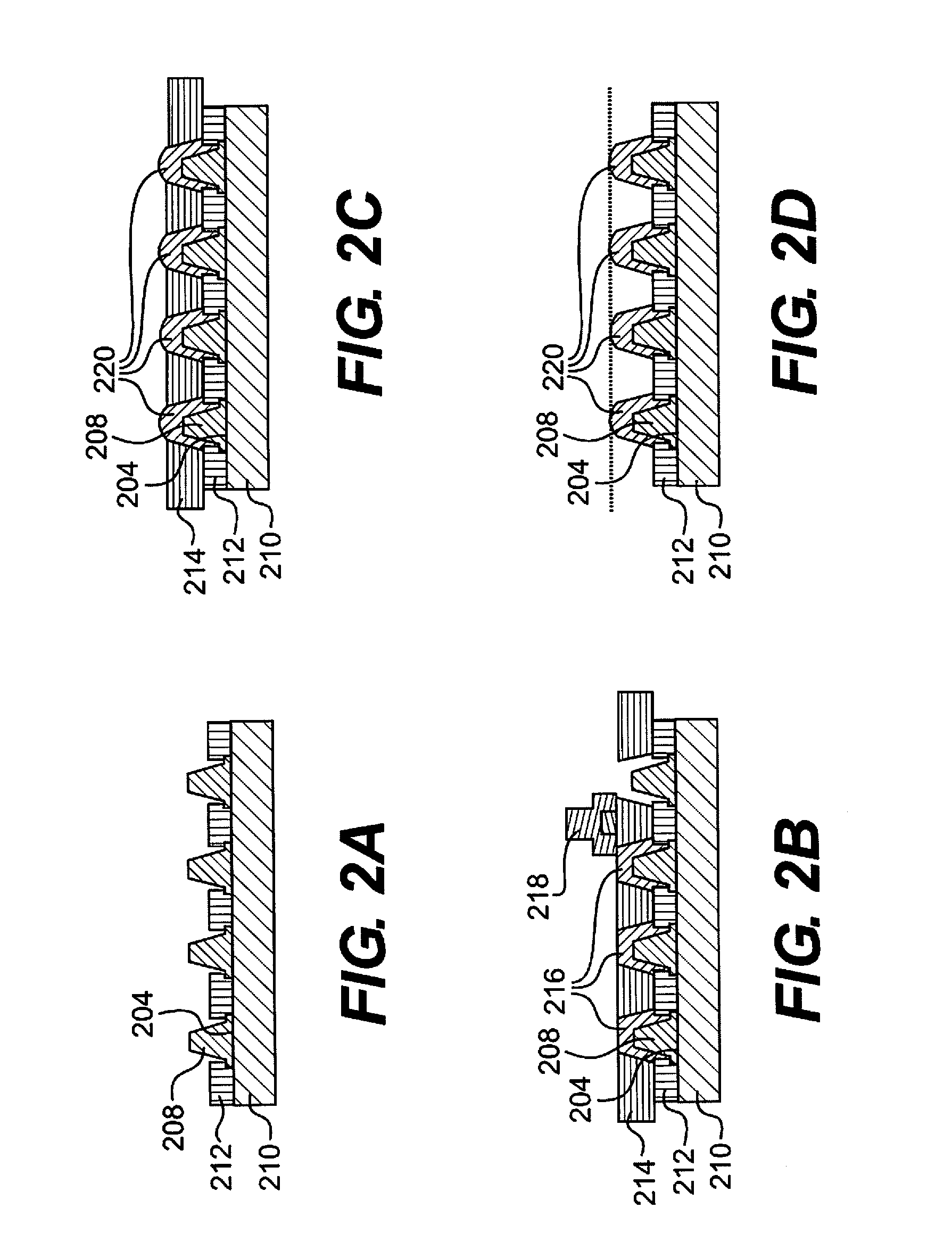
[0066]The present invention comprises methods of forming solder bumps on Cu posts positioned on the organic substrate of a semiconductor / organic substrate device by means of injection molding of molten solder through a reusable mask positioned on the device. We refer to semiconductors, wafers, dies and chips in our description of the invention and intend that these terms are to be considered as interchangeable, as are the terms copper posts...


PUM


Abstract

A method comprises forming semiconductor flip chip interconnects having electrical connecting pads and electrically conductive posts terminating in distal ends operatively associated with the pads. We solder bump the distal ends by injection molding, mask the posts on the pads with a mask having a plurality of through hole reservoirs and align the reservoirs in the mask to be substantially concentric with the distal ends. Injecting liquid solder into the reservoirs and allowing it to cool provides solidified solder on the distal ends, which after mask removal produces a solder bumped substrate which we position on a wafer to leave a gap between the wafer and the substrate. The wafer has electrically conductive sites on the surface for soldering to the posts. Abutting the sites and the solder bumped posts followed by heating joins the wafer and substrate. The gap is optionally filled with a material comprising an underfill.

Description

FIELD OF THE INVENTION[0001]The field of the invention comprises electrical interconnects between semiconductor devices and substrates on which such devices are packaged, and more particularly, injection molded solder techniques used to make these interconnects.BACKGROUND OF THE INVENTION[0002]For solder flip chip assembly of a first level package or device, the solder interconnects are formed by joining solder bumps on the chip with solder bumps on the substrate. The solder bumps on the substrate help compensate for chip bump height variations and substrate warpage. Flip chip technology allows the largest numbers of inputs / outputs (“I / Os”) for the smallest footprint of the chip. This enables manufacturing small packages known in the art as chip-scale packages.[0003]IBM introduced this technology in the early 1960's with the solid logic technology in their IBM System / 360™. It extended interconnection capabilities beyond existing wire-bonding techniques, allowing the area array solde...

Claims


Application Information

Patent Timeline
Patent Type & Authority Applications(United States)
IPC IPC(8): H01L23/00
CPCH01L24/81H01L24/11H01L21/4853H01L21/563H01L23/49816H01L24/13H01L24/16H01L24/73H01L24/83H01L24/92H01L2224/1132H01L2224/1134H01L2224/13022H01L2224/13076H01L2224/131H01L2224/13147H01L2224/1403H01L2224/14051H01L2224/14131H01L2224/14135H01L2224/1601H01L2224/16225H01L2224/16227H01L2224/45124H01L2224/73104H01L2224/73204H01L2224/81192H01L2224/81193H01L2224/81203H01L2224/81815H01L2224/83191H01L2224/83192H01L2224/83203H01L2224/9211H01L2924/00013H01L2924/00014H01L2924/01029H01L2924/10253H01L2924/1461H01L2924/15747H01L2924/181H01L2924/3841H01L2924/00012H01L2224/81H01L2224/83H01L2224/13099H01L2224/13599H01L2224/05599H01L2224/05099H01L2224/29099H01L2224/29599H01L2924/014H01L2924/3512H01L2924/00H01L2224/48H01L23/562H01L2224/11312H01L2224/11462H01L2924/01013H01L2924/01079H01L2924/14
Inventor NAH, JAE-WOONGSHIH, DA-YUAN
Owner INT BUSINESS MASCH CORP
Why Eureka
Try Eureka