
Dual-gate driven lateral pixel arrangement structure and display panel

a lateral pixel arrangement and dual-gate technology, applied in the field of display technologies, can solve the problems of increased system cost, difficult manufacturing process of conventional thin film transistors, and serious colour offset and chromatic aberration

Active Publication Date: 2014-03-20
SHANGHAI AVIC OPTOELECTRONICS
View PDF7 Cites 13 Cited by
  • Summary
  • Abstract
  • Description
  • Claims
  • Application Information

AI Technical Summary

Benefits of technology

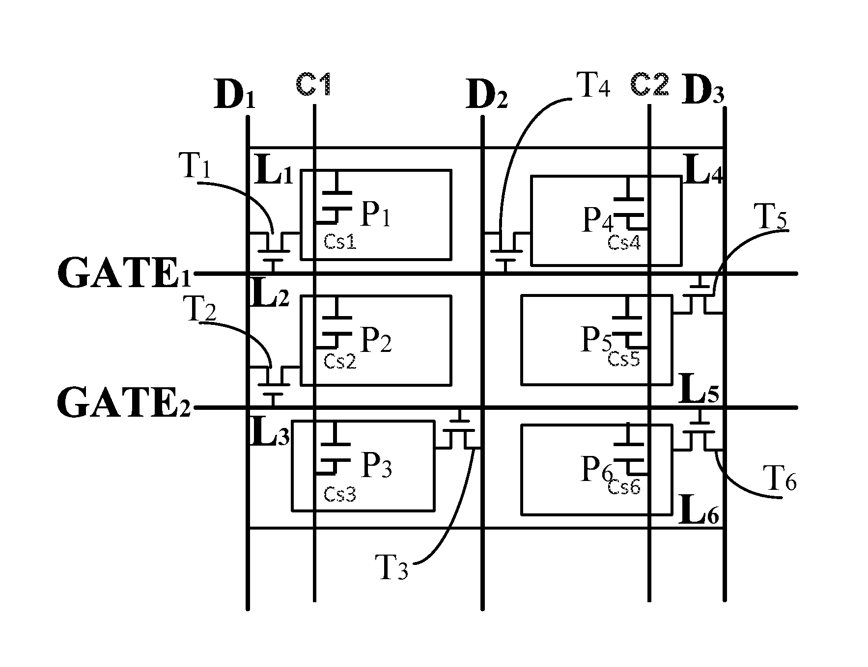
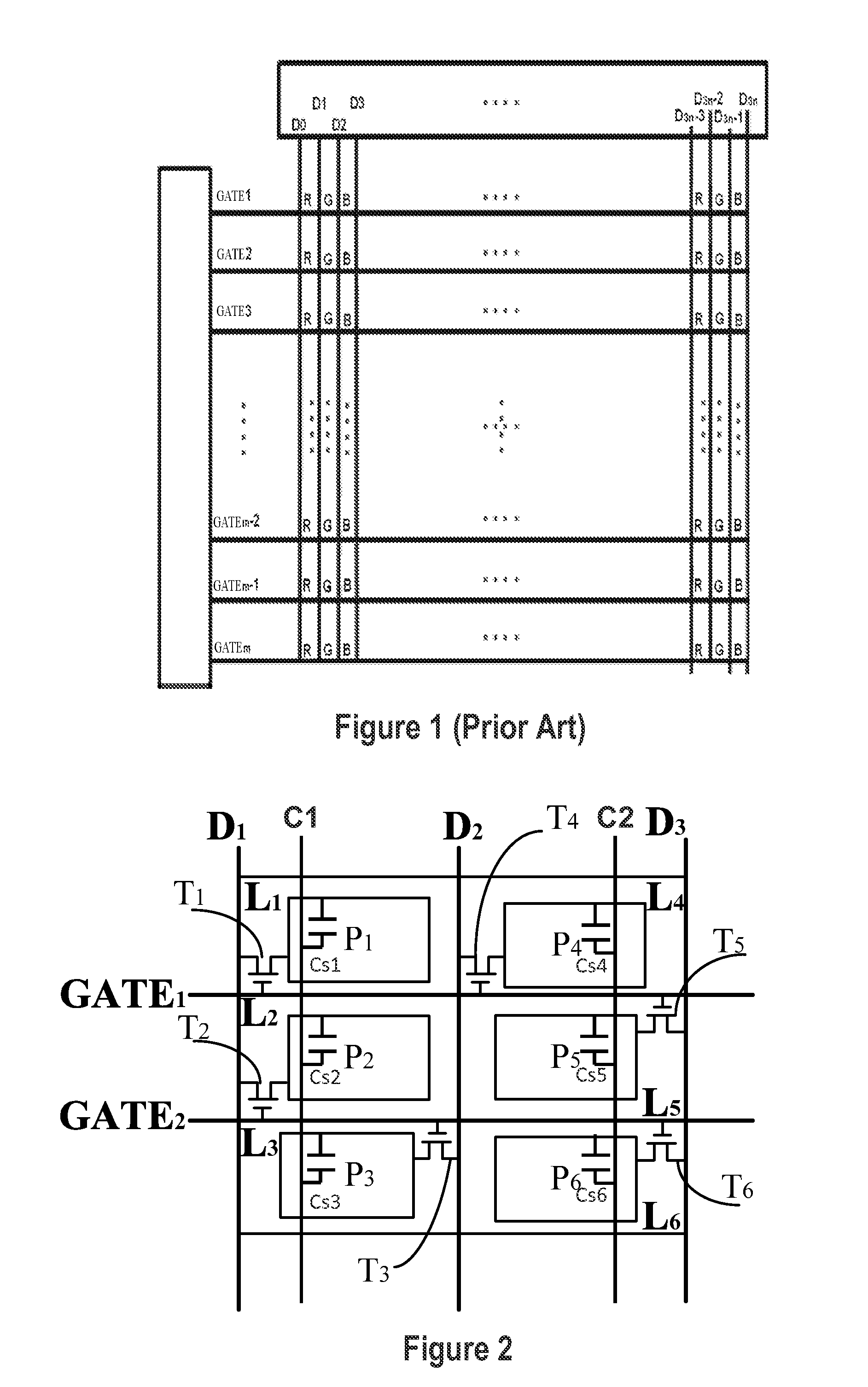
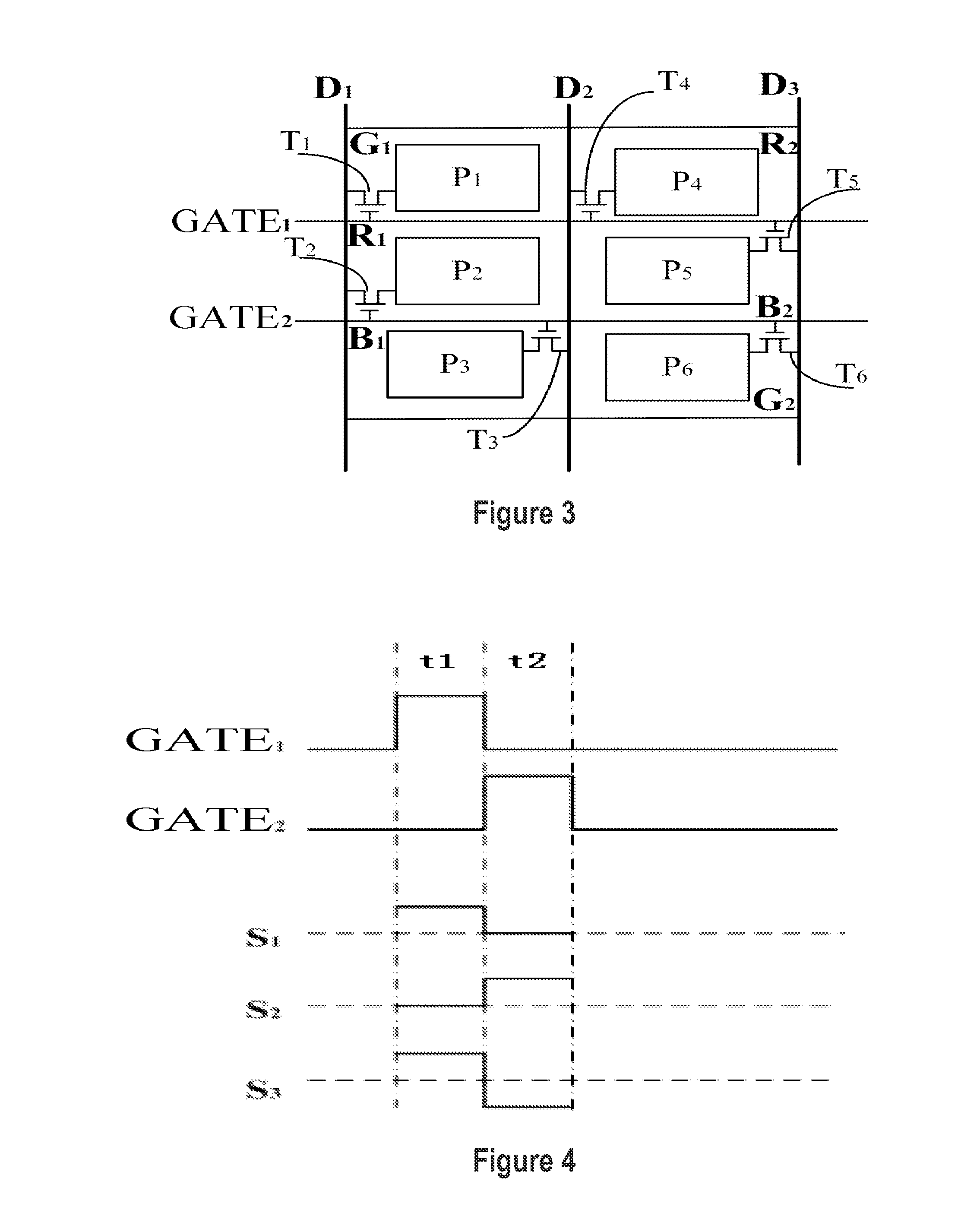
The present invention provides a dual-gate-driven lateral pixel arrangement structure for a high resolution display panel. This structure requires only about half the number of gate lines and data lines compared to a single-gate-driven lateral pixel arrangement mode. As a result, the driving time for each gate line is reduced to one-half, and the manufacturing process for conventional TFT can also meet the requirements for a high resolution display panel.

Problems solved by technology

Because of a positioning error between the glass plate on which the raster grids are provided and the display panel during assembly, the raster grids may block a certain colour, for example, a part of the area of the red sub-pixel region may be covered, thus causing a serious colour offset and chromatic aberration.
In such an arrangement mode, a buffer needs to be added to the driving circuit for the lateral-to-vertical conversion of a display signal, but this will greatly increase the system costs.
Because the number of the gate lines is three times that of single-gate-driven lateral pixel arrangement mode in which a vertical screen is laterally utilized, and the driving time of each gate line is shortened to one-third of that of single-gate-driven lateral pixel arrangement mode in which a vertical screen is laterally utilized; in the case of a high resolution display, it is difficult for the manufacturing process of conventional thin film transistors (TFTs) to meet the driving requirements.

Method used


Image

  • Dual-gate driven lateral pixel arrangement structure and display panel
  • Dual-gate driven lateral pixel arrangement structure and display panel
  • Dual-gate driven lateral pixel arrangement structure and display panel

Examples


Embodiment Construction

[0032]Embodiments of the present invention will be described fully below in conjunction with the accompanying drawings. Those of ordinary skill in the art will appreciate that the following description of the present invention is illustrative only and not in any way limiting. Other embodiments of the invention will readily suggest themselves to a person of ordinary skill in the art after a perusal of this disclosure.

[0033]One embodiment of the invention provides a dual-gate-driven lateral pixel arrangement structure including a plurality of pixel units. Each of the pixel units may include a first gate line and a second gate line, and three data lines (a first data line, a second data line and a third data line) that are arranged in sequence. In an embodiment, the two gate lines are disposed on a substrate and arranged in parallel along a first direction, and the three data lines are disposed on the substrate and arranged in parallel along a second direction. The two gate lines cross...


PUM

PropertyMeasurementUnit
light transmissionaaaaaaaaaa
timeaaaaaaaaaa
sizeaaaaaaaaaa

Abstract

A dual-gate-driven lateral pixel arrangement structure includes two horizontally adjacent primary pixel regions having each three vertically adjacent secondary pixel regions forming a grid of six secondary pixel regions, and six thin-film transistors disposed in each of the six secondary pixel areas. The structure also includes two gate lines and three data lines crossing each other and electrically isolated from each other. Each data line is connected to the source of two thin-film transistors having the gate connected to a different gate line. The two gate lines are interposed between the three secondary pixel regions or arranged along a side or opposite sides of the primary pixel regions in a first direction. The three data lines are arranged between the primary pixel regions and along a side or opposite sides of the primary pixel regions in a second direction different from the first direction.

Description

CROSS-REFERENCES TO RELATED APPLICATIONS[0001]This application claims priority to and is a continuation-in-part of PCT / CN2012 / 075993, filed on May 24, 2012 and entitled “DUAL-GATE-DRIVEN LATERAL PIXEL ARRANGEMENT STRUCTURE AND DISPLAY PANEL”, which application claims the benefit of Chinese Patent Application No. 201110231785.X, filed with the Chinese Patent Office on Aug. 12, 2011, and entitled “DUAL-GATE-DRIVEN LATERAL PIXEL ARRANGEMENT STRUCTURE AND DISPLAY PANEL”, the contents of which are incorporated herein by reference in their entirety.FIELD OF THE INVENTION[0002]The present invention relates to display technologies, and more particularly, to a dual-gate-driven lateral pixel arrangement structure and a display panel of using the same.BACKGROUND OF THE INVENTION[0003]In the prior art, three sub-pixel regions for display in red (R), green (G) and blue (B) are arranged from left to right in a primary pixel region of a display panel, each primary pixel region has a square or circ...

Claims


Application Information

Patent Timeline
Patent Type & Authority Applications(United States)
IPC IPC(8): G02F1/1362G09G3/36
CPCG02F1/136286G09G3/3648G02F1/13624G09G2300/0426G02F1/133G09G3/36
Inventor XIA, ZHIQIANGCHEN, CHENHUANG, ZHONGSHOUZHOU, SISI
Owner SHANGHAI AVIC OPTOELECTRONICS
Learn More