Eureka AIR delivers breakthrough ideas for toughest innovation challenges, trusted by R&D personnel around the world.

Pixel Cell and Active Matrix Liquid Crystal Display

Active Publication Date: 2014-03-20
TCL CHINA STAR OPTOELECTRONICS TECH CO LTD
View PDF3 Cites 0 Cited by
  • Summary
  • Abstract
  • Description
  • Claims
  • Application Information

AI Technical Summary

Benefits of technology

The patent text describes an active matrix liquid crystal display with a special design to reduce unwanted electrical effects. The display includes a non-display area and a display area with multiple pixel cells. Each pixel cell has a first and second scanning line that runs parallel to each other, and a data line that crosses the first and second scanning lines. The pixel electrode is connected to the first and second scanning lines, as well as the data line. The thin film transistor set, which includes a first and second thin film transistor, is connected to the first and second scanning lines, the data line, and the pixel electrode. The thin film transistor set also has a parasitic capacitance that satisfies a certain equation, which results in a change in capacitance that is opposite to the change in capacitance caused by the overlap of the first thin film transistor's gate and drain. The change in capacitance caused by both components is equal to each other, which helps to reduce unwanted electrical effects.

Problems solved by technology

Thus, the display performance is not good due to Mura effect, image flicker, and so on.

Method used


Image

  • Pixel Cell and Active Matrix Liquid Crystal Display
  • Pixel Cell and Active Matrix Liquid Crystal Display
  • Pixel Cell and Active Matrix Liquid Crystal Display

Examples


Embodiment Construction

[0026]Embodiments of the invention will now be described more fully hereinafter with reference to the accompanying drawings, in which embodiments of the invention are shown.

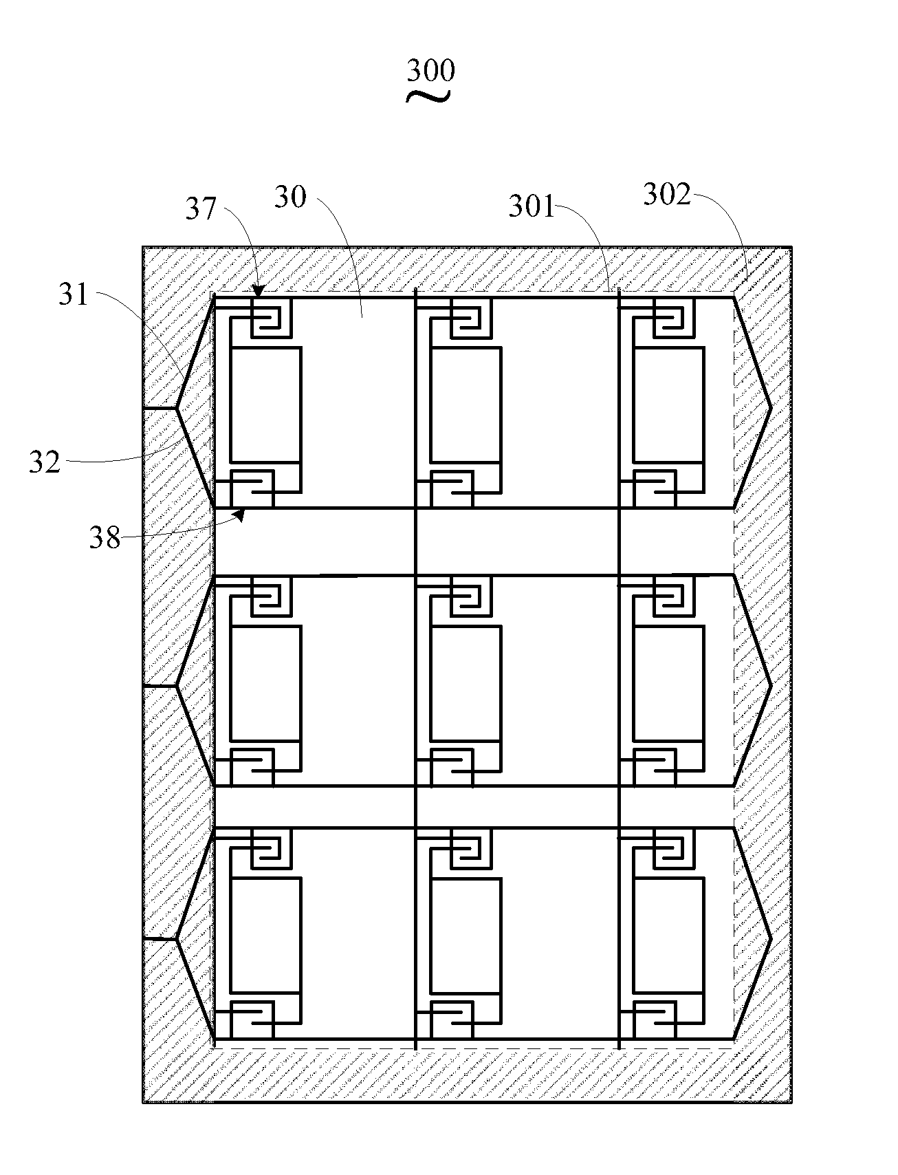
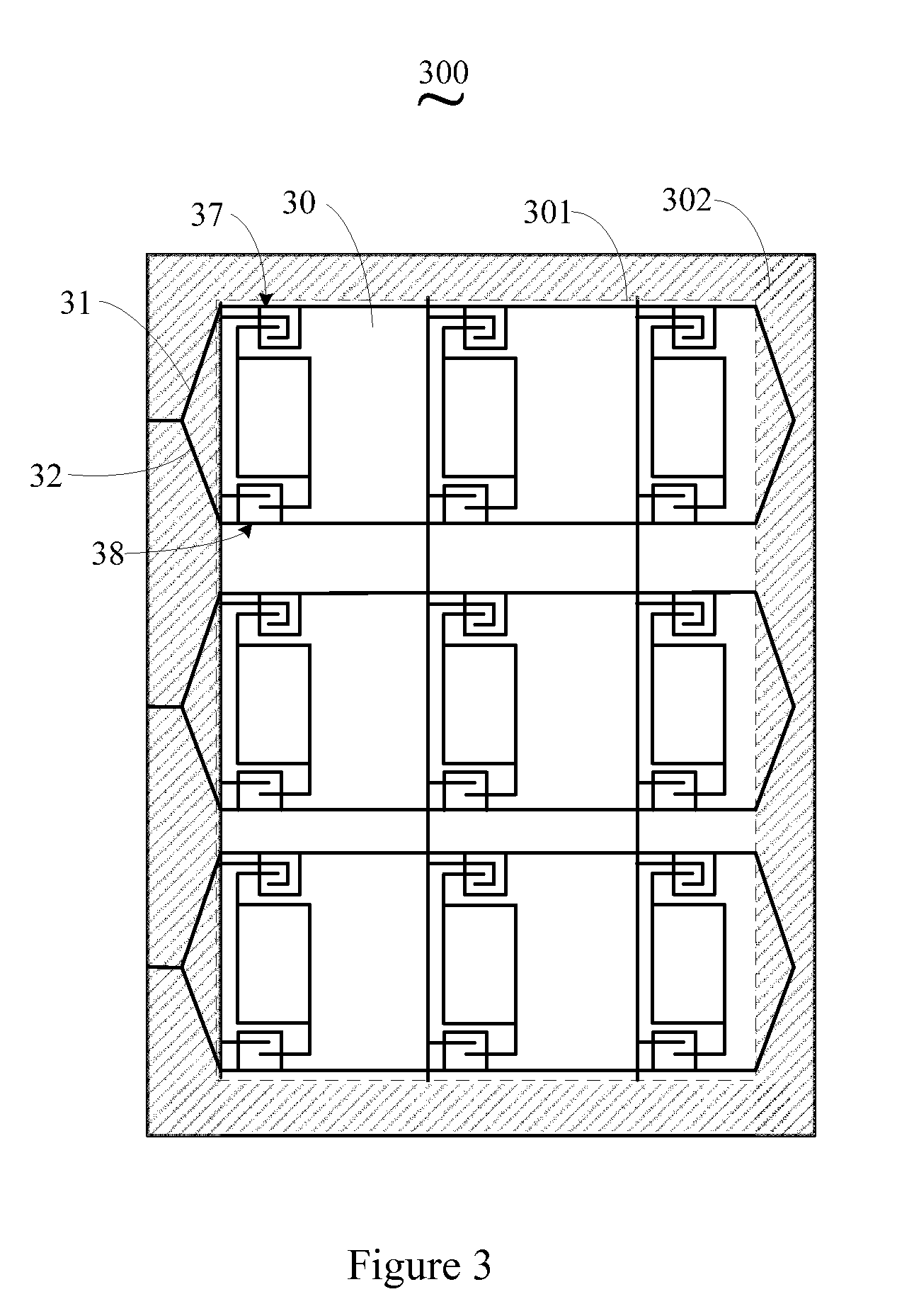
[0027]FIG. 3 is a schematic view of the AMLCD in accordance with one embodiment. The AMLCD 300 includes a display area 301 and a non-display area 302.

[0028]In the embodiment, the display area 301 includes a plurality of pixel cells 30.

[0029]FIG. 4 is a schematic view of one pixel cell of the AMLCD under an ideal exposure scenario. As shown in FIG. 4, the pixel cells 30 include a first scanning line 31, a second scanning line 32, a data line 33, a pixel electrode 35 and a thin film transistor set 36.

[0030]The first scanning line 31 and the second scanning line 32 are arranged spaced apart from each other in the display area 301 and are parallel to each other. The data line 33 respectively crosses the first scanning line 31 and the second scanning line 32 at right angles. The pixel electrode 35 electrically connect...


PUM


Abstract

A pixel cell and an active matrix liquid crystal display are disclosed. The pixel cell includes a first scanning line, a second scanning line, and a thin film transistor set. The thin film transistor set includes a first thin film transistor and a second thin film transistor. The parasitic capacitance Cgd of the thin film transistor set satisfies the equation: Cgd=C1+C2. Wherein the change in capacitance of both c1 and c2 are inverse to each other by the same amount such that summation of a value of capacitance change in both c1 and c2 is equal to zero. In this way, the display detects result from different values of the parasitic capacitance of the pixel cells in different locations are overcome.

Description

BACKGROUND OF THE INVENTION[0001]1. Field of the Invention[0002]Embodiments of the present disclosure relate to display technology, and more particularly to a pixel cell and an active matrix liquid crystal display (AMLCD).[0003]2. Discussion of the Related Art[0004]FIG. 1 is a schematic view of a typical AMLCD. As shown in FIG. 1, the AMLCD 10 includes a plurality of pixel cells. Each pixel cell includes a thin-film transistor. For example, the pixel cell P1 includes the thin-film transistor T1, and the pixel cell P2 includes the thin-film transistor T2.[0005]In the manufacturing process of the AMLCD 10, the overlay shift may exist between the drain and the gate of the thin-film transistor in different exposure locations due to exposure precision. Thus, the thin-film transistor in different locations may have different parasitic capacitance.[0006]FIG. 2 is an enlarged view of the thin-film transistor T1 and thin-film transistor T2 of FIG. 1. As shown in FIG. 2, the parasitic capacit...

Claims


Application Information

Patent Timeline
IPC IPC(8): G02F1/1343
CPCG02F1/134336G02F1/136227G02F1/13624
Inventor WANG, JINJIE
Owner TCL CHINA STAR OPTOELECTRONICS TECH CO LTD
Why Eureka
Eureka Blog
Learn More