Plasma processing method and plasma processing device

Active Publication Date: 2014-04-17
ADVANCED MICRO FAB EQUIP INC CHINA
View PDF5 Cites 22 Cited by
  • Summary
  • Abstract
  • Description
  • Claims
  • Application Information

AI Technical Summary

Benefits of technology

[0014]In the pulse plasma processing device controlled by the method of the invention, the matching of the fast alternating impedance can be achieved without making great changes to the hardware. Before the pulse processing stage, the variable frequency RF power supply is tuned within sever

Problems solved by technology

In the traditional art, auto frequency tuning (AFT) in the match circuit or the RF power supply is employed, and since

Method used


Image

  • Plasma processing method and plasma processing device
  • Plasma processing method and plasma processing device
  • Plasma processing method and plasma processing device

Examples


first embodiment

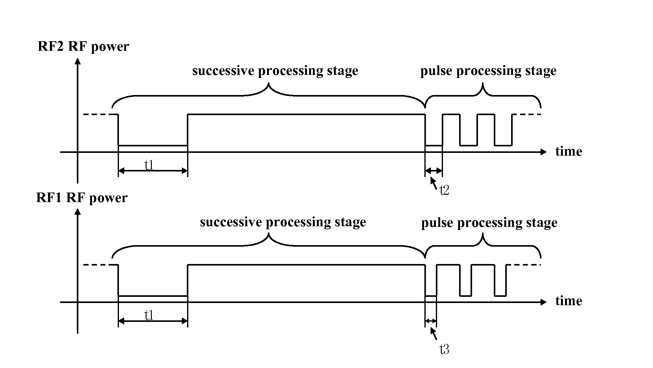
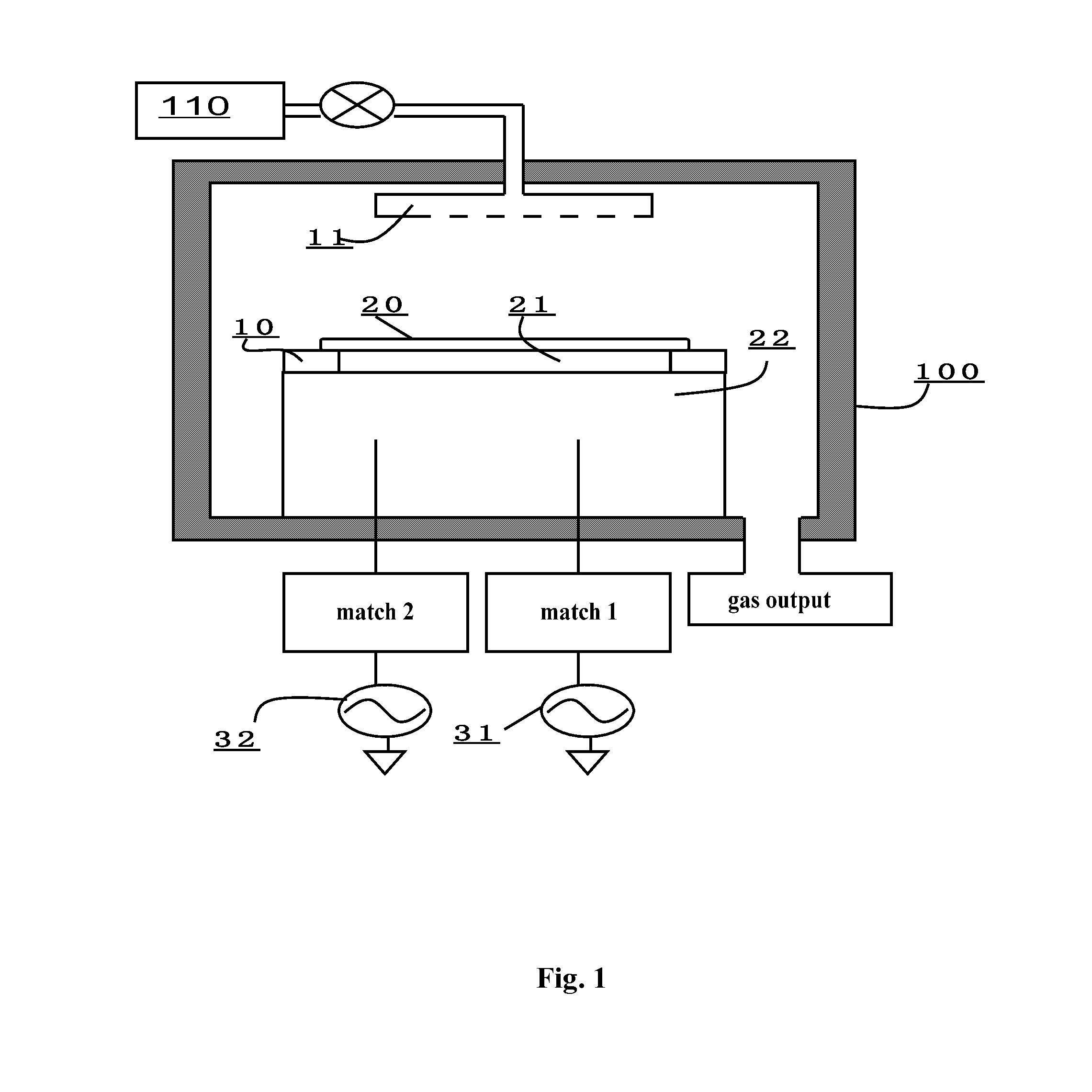
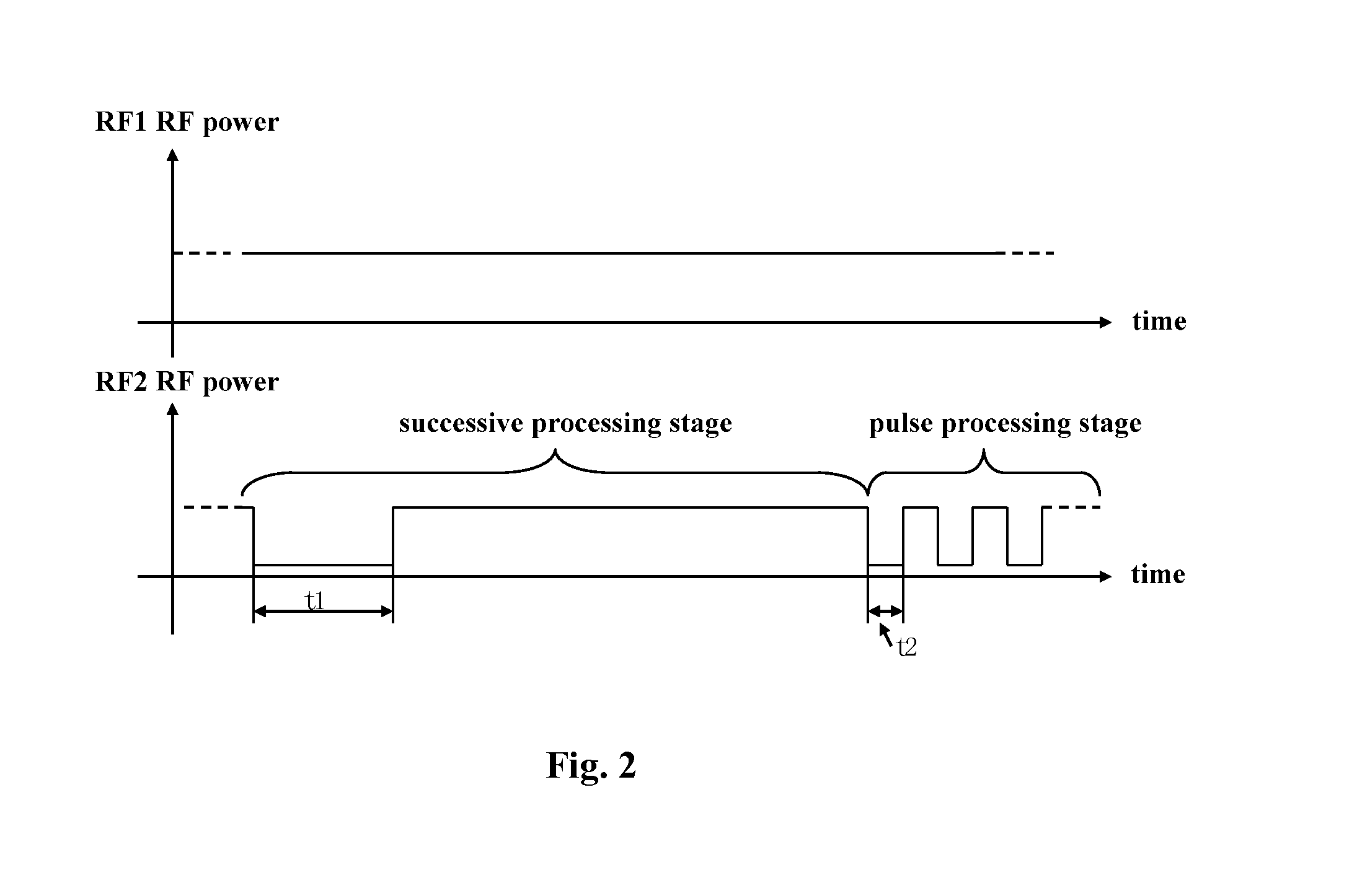
[0021]FIG. 2 illustrates the invention. The Radio Frequency (RF) powers of the first RF power supply RF1 and the second RF power supply RF2 in FIG. 2 respectively represent the output powers of the first RF power supply 31 and the second RF power supply 32 in FIG. 1. In the plasma processing, the plasma is firstly ignited, then after some possible transitional steps, the main plasma processing step, i.e., the successive processing stage, is carried out. Since steps such as the plasma igniting step are traditional steps in the prior art and have no direct influence on present invention, they are shown only by a dotted line in FIG. 2. Therefore, in the successive processing stage, both the first RF power supply RF1 and the second RF power supply RF2 are in a high power state, until an optical detector in the reaction chamber detects that the plasma processing reaches a certain level, for example in the plasma etching it is found that more than 70% of a particular material layer has be...

second embodiment

[0025]In the invention, when the low power output of the pulse RF power supply is greater than zero, a variable frequency RF power supply other than said pulse RF power supply may be employed to adjusted the output frequency and obtain the match frequency, or the pulse RF power supply itself may be employed to adjusted the output frequency and obtain the match frequency. When the low power output of the pulse RF power supply is zero, i.e., the output of the pulse RF power supply is turned off, the match frequency can only be obtained by adjusting the output frequency of other variable frequency RF power supply. Therefore, in the second embodiment shown in FIG. 3, if the output powers of RF1 and RF2 are small but greater than zero in the time period of t1, the match frequency can be obtained by adjusting the RF frequency output of RF1, or the optimal match frequency may be obtained by adjusting the output frequencies of both RF1 and RF2.

[0026]In the invention, besides using two RF po...


PUM


Abstract

A plasma processing method for a plasma processing device is provided. The plasma processing device includes a reaction chamber, multiple Radio Frequency (RF) power supplies with different RF frequency outputs apply RF electric fields to the reaction chamber, the output of at least one pulse RF power supply has multiple output states, and the processing method includes a match frequency obtaining step and a pulse processing step. In the match frequency obtaining step, the output state of the pulse RF power supply is switched to make the reaction chamber have multiple impedances to simulate the impedances in the pulse processing step. The output frequencies of the variable frequency RF power supply are adjusted to match the simulated impedances. The adjusted output frequencies are stored as match frequencies. In the subsequent pulse processing step, the fast switched impedances are instantly matched by the stored match frequencies.

Description

[0001]This application claims the priority of Chinese Patent Application No. 201210393470.X, entitled “PLASMA PROCESSING METHOD AND PLASMA PROCESSING DEVICE”, filed with the Chinese State Intellectual Property Office on Oct. 16, 2012, the content of which is incorporated herein by reference in its entirety.FIELD OF THE INVENTION[0002]The invention relates to a plasma processing method and a plasma processing device, and in particular to a Radio Frequency (RF) power supply which provides RF power to the plasma processing device and a method for controlling the RF power supply.BACKGROUND OF THE INVENTION[0003]In the existing semiconductor processing, plasma processing apparatuses are widely used to process semiconductor wafers, so as to obtain micro dimension semiconductor devices and conductive connections. The plasma apparatus usually includes Capacitively Coupled Plasma (CCP) reaction chamber or Inductively Coupled Plasma (ICP) reaction chamber. These apparatuses usually have two R...

Claims


Application Information

Patent Timeline
IPC IPC(8): H01L21/3065
CPCH01L21/3065H01J37/32091H01J37/32165H01J37/32183H05H1/46
Inventor XU, LEINI, TUQIANGXI, ZHAOHUI
Owner ADVANCED MICRO FAB EQUIP INC CHINA
Why Eureka
Try Eureka