Epitaxy Technique for Growing Semiconductor Compounds

a technology of epitaxial growth and semiconductor layers, applied in semiconductor/solid-state device manufacturing, semiconductor devices, electrical equipment, etc., can solve the problem that the approach does not enable epitaxial growth of nitride-based semiconductor layers with uniform composition

Active Publication Date: 2014-04-24
SENSOR ELECTRONICS TECH
View PDF12 Cites 34 Cited by
  • Summary
  • Abstract
  • Description
  • Claims
  • Application Information

AI Technical Summary

Problems solved by technology

While the superlattice approaches allow some control of tensile and compressive stresses in epitaxially grown nitride semiconductor layers, the approaches do not enable epitaxial growth of nitride based semiconductor layers with uniform composition.

Method used


Image

  • Epitaxy Technique for Growing Semiconductor Compounds
  • Epitaxy Technique for Growing Semiconductor Compounds
  • Epitaxy Technique for Growing Semiconductor Compounds

Examples


Embodiment Construction

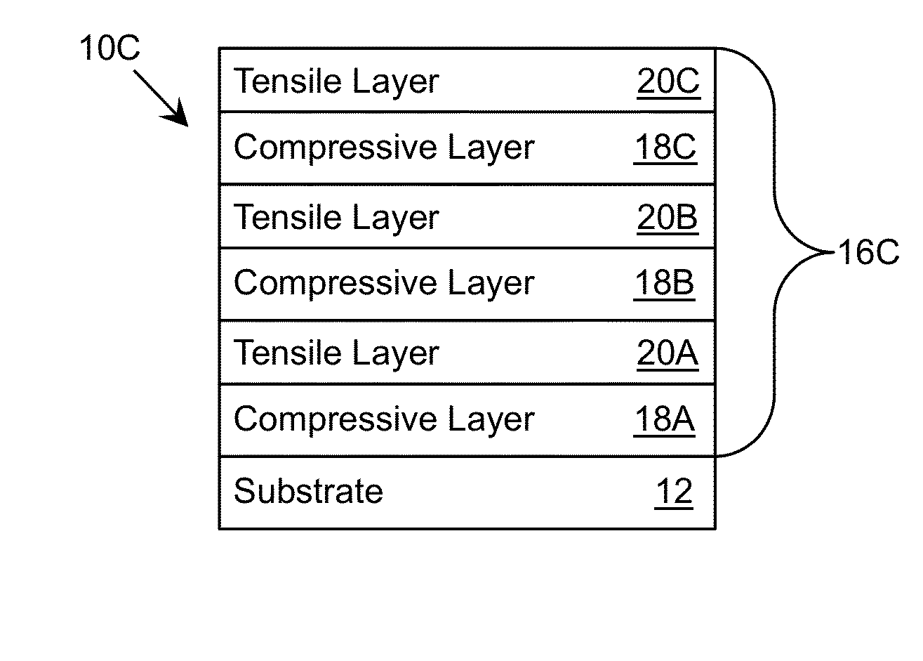
[0025]As indicated above, aspects of the invention provide a solution for fabricating a semiconductor structure. The semiconductor structure includes a plurality of semiconductor layers grown over a substrate using a set of epitaxial growth periods. During each epitaxial growth period, a first semiconductor layer having one of: a tensile stress or a compressive stress is grown followed by growth of a second semiconductor layer having the other of: the tensile stress or the compressive stress directly on the first semiconductor layer. In this manner, the overall residual stress for the plurality of semiconductor layers can be approximately zero, which can result in the semiconductor structure having a reduced number of cracks and / or threading dislocations than prior art approaches. As used herein, unless otherwise noted, the term “set” means one or more (i.e., at least one) and the phrase “any solution” means any now known or later developed solution.

[0026]Aspects of the invention ar...


PUM


Abstract

A solution for fabricating a semiconductor structure is provided. The semiconductor structure includes a plurality of semiconductor layers grown over a substrate using a set of epitaxial growth periods. During each epitaxial growth period, a first semiconductor layer having one of: a tensile stress or a compressive stress is grown followed by growth of a second semiconductor layer having the other of: the tensile stress or the compressive stress directly on the first semiconductor layer.

Description

REFERENCE TO RELATED APPLICATIONS[0001]The current application claims the benefit of co-pending U.S. Provisional Application No. 61 / 566,606, titled “Epitaxy Technique for Growing Low Stress Nitride-Based Semiconductor Compounds,” which was filed on 3 Dec. 2012, and which is hereby incorporated by reference.GOVERNMENT LICENSE RIGHTS[0002]This invention was made with government support under contract no. W911 NF-10-2-0023 awarded by the Defense Advanced Research Projects Agency (DARPA). The government has certain rights in the invention.TECHNICAL FIELD[0003]The disclosure relates generally to growing semiconductor compounds, and more particularly, to an epitaxy technique for such growth, which can result in a low stress compound.BACKGROUND ART[0004]For light emitting devices, such as light emitting diodes (LEDs) and especially deep ultraviolet LEDs (DUV LEDs), minimizing a dislocation density and a number of cracks in the semiconductor layers increases the efficiency of the device. To...

Claims


Application Information

Patent Timeline
Patent Type & Authority Applications(United States)
IPC IPC(8): H01L33/06H01L29/15H01L21/02
CPCH01L33/06H01L29/151H01L21/02433H01L21/0237H01L21/02458H01L21/02507H01L21/0254H01L21/0262H01L33/007H01L33/025
Inventor JAIN, RAKESHSUN, WENHONGYANG, JINWEISHATALOV, MAXIM S.DOBRINSKY, ALEXANDERGASKA, REMIGIJUSSHUR, MICHAEL
Owner SENSOR ELECTRONICS TECH
Why Eureka
Try Eureka