Semiconductor package including leadframe roughened with chemical etchant to prevent separation between leadframe and molding compound

a technology of chemical etchant and semiconductor chip, which is applied in the direction of semiconductor/solid-state device details, semiconductor devices, electrical apparatus, etc., can solve the problems of corroding the metal components of the package and the semiconductor chip, fractured wire bonds, and stress at the interface between metal and plastic, so as to reduce the tendency of the leadframe and enhance the adhesion

Inactive Publication Date: 2006-05-11
UTAC HEADQUARTERS PTE LTD
View PDF16 Cites 121 Cited by
  • Summary
  • Abstract
  • Description
  • Claims
  • Application Information

AI Technical Summary

Benefits of technology

[0011] The roughening of the leadframe causes the surface of the metal to be textured with asperities and, in addition, a coating may be formed on the surface of the leadframe. The roughened surface and the coating enhance the adhesion between the leadframe and the molten plastic during the encapsulation process. This enhanced adhesion reduces the tendency of the leadframe and plastic to separate as a result of the differing thermal-expansion rates between the metal and the package capsule.

Problems solved by technology

As a result, as the package cycles between high and low temperatures, stresses are created at the interfaces between the metal and plastic.
Over time, this can lead to fractured wire bonds.
This moisture can corrode the metal components of the package and semiconductor chip.
If the package is subjected to freezing temperatures, the moisture can expand and cause separation between the plastic molding compound and the metal.
Conversely, if the package is exposed to very high temperatures, the moisture can turn to steam and likewise cause separation or, in extreme cases, cause the package to experience a “popcorn” effect.
This situation as worsened recently as a result of the restrictions on the use of lead in the solder that is used to make the connections between the lead fingers of the semiconductor package and the PCB.

Method used


Image

  • Semiconductor package including leadframe roughened with chemical etchant to prevent separation between leadframe and molding compound
  • Semiconductor package including leadframe roughened with chemical etchant to prevent separation between leadframe and molding compound
  • Semiconductor package including leadframe roughened with chemical etchant to prevent separation between leadframe and molding compound

Examples


Embodiment Construction

[0023] We have found that the problems described above can be greatly reduced by using a chemical etching process to roughen the surface of the leadframe. Roughening the leadframe enhances the adhesion between the metal surface of the leadframe and the molten plastic during the process of encapsulation and reduces the separation that occurs because of thermal expansion and moisture ingress into the package.

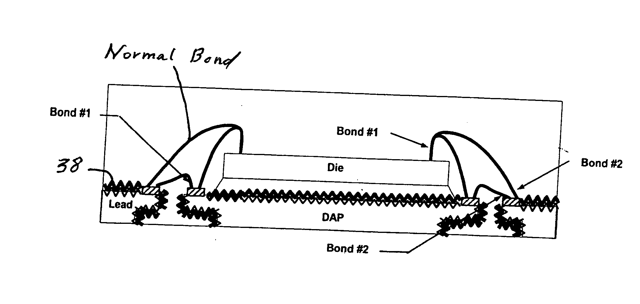
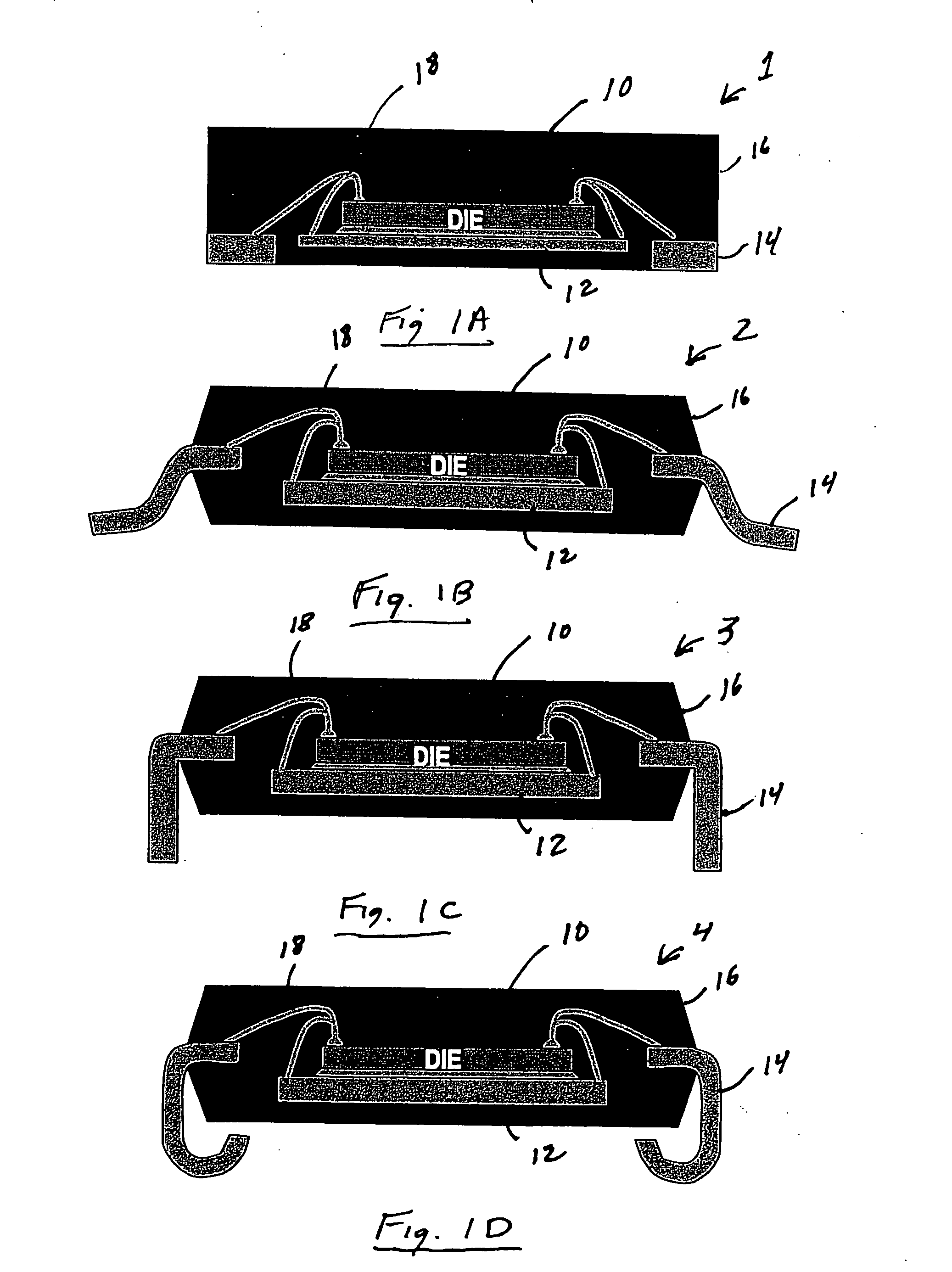
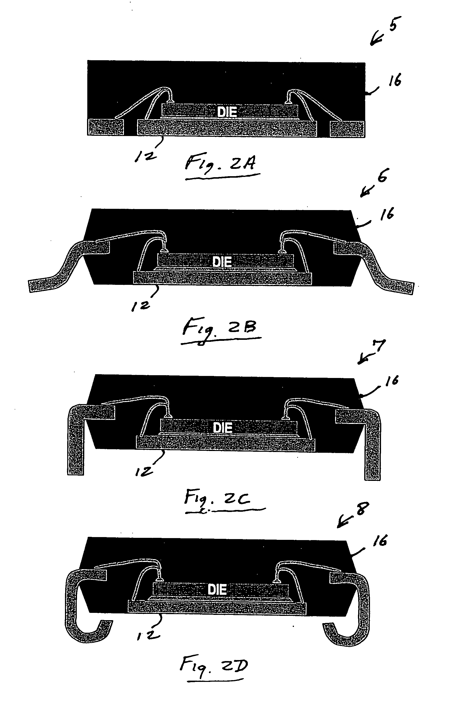
[0024] Copper alloy leadframes are normally plated with silver (Ag) or an alloy in order to facilitate the bonding of wires to the leadframe. Alloys that can be used as alternative plating materials include Ni / Au, Ni / Pd, Ni / Pd / Au, and Ni / Pd / Au alloys. The plating covers the areas of the lead fingers or die-attach pad where electrical connections are to be made to other components, typically by wire bonding. FIGS. 3A-3H are top views of a dual side package 20 having a die-attach pad 22 and lead fingers (or metal contacts if the package is unleaded) 24A-24H, with the semiconductor ...


PUM

PropertyMeasurementUnit
mean peak-to-valley heightaaaaaaaaaa
heightaaaaaaaaaa
profile valley depthaaaaaaaaaa

Abstract

A semiconductor package contains a metal leadframe that has been specially treated by roughening it with a chemical etchant. The roughening process enhances the adhesion between the leadframe and the molten plastic during the encapsulation of the leadframe and thereby reduces the tendency of the package to separate when exposed to moisture and numerous temperature cycles. In one embodiment, the leadframe made of copper is roughened with a chemical etchant that contains sulfuric acid and hydrogen peroxide.

Description

[0001] This application is a continuation of application Ser. No. 10 / 622,346, filed Jul. 19, 2003, which is incorporated herein by reference in its entirety.FIELD OF THE INVENTION [0002] This invention relates to semiconductor packages which contain a semiconductor die, a leadframe for connecting terminals on the die to external circuitry, and an encapsulant for enclosing and protecting the die. BACKGROUND OF THE INVENTION [0003] Semiconductor dice are normally packaged in a plastic capsule to protect them from physical damage. Connections are made to external circuitry, such as a printed circuit board (PCB), by means of metal pieces, called “lead fingers,” that protrude from the capsule and can be soldered or otherwise connected electrically. Alternatively, in a “no lead” package the metal pieces have faces that are flush with the surfaces of the capsule. [0004]FIGS. 1A-1D show four configurations of a semiconductor package. Each package contains a semiconductor die 10, a die-attac...

Claims


Application Information

Patent Timeline
Patent Type & Authority Applications(United States)
IPC IPC(8): H01L23/495
CPCH01L21/4835H01L23/3142H01L23/495H01L23/49582H01L24/48H01L24/49H01L2224/45124H01L2224/45144H01L2224/48091H01L2224/48247H01L2224/48257H01L2224/48465H01L2224/48599H01L2224/48699H01L2224/49109H01L2224/4911H01L2924/01011H01L2924/01013H01L2924/01014H01L2924/01027H01L2924/01028H01L2924/01029H01L2924/01046H01L2924/01047H01L2924/01078H01L2924/01079H01L2924/01082H01L2924/01088H01L2924/014H01L2924/19107H01L2924/01006H01L2924/01019H01L2924/01033H01L24/32H01L2224/32245H01L2224/73265H01L2924/15747H01L2224/8301H01L2224/8501H01L2924/00014H01L2924/00012H01L2924/00H01L2924/181H01L2224/85207H01L2924/18301H01L2224/85439H01L2224/85455H01L2224/85664H01L2224/05624H01L2224/85447H01L2224/85444H01L2224/83385H01L2924/00015H01L2224/45099
Inventor SIRINORAKUL, SARAVUTHLAYSON, ARLENE V.NONDHASITTHICHAI, SOMCHAICHUA, YEE HEONG
Owner UTAC HEADQUARTERS PTE LTD
Why Eureka
Try Eureka