Image Sensor

a technology of image sensor and image, applied in the field of image sensor, can solve the problems of disadvantageously serious deterioration of image quality of the corresponding region(s), image sensor is not capable of treating or processing all information of an actual scene, etc., and achieves the effects of low luminance, reduced generation of dark current, and wide dynamic rang

Inactive Publication Date: 2014-05-01
DONGBU HITEK CO LTD
View PDF6 Cites 45 Cited by
  • Summary
  • Abstract
  • Description
  • Claims
  • Application Information

AI Technical Summary

Benefits of technology

[0010]It is one object of the present invention to provide an image sensor that accomplishes wide dynamic range (WDR) and reduces generation of dark current at a low luminance.

Problems solved by technology

The image sensor is not capable of treating or processing all information of an actual scene since the obtainable dynamic region is considerably smaller than the dynamic region of the actual image.
In particular, when an image is obtained under an environment such as backlight, the image sensor cannot sufficiently obtain information of both the brightest region and the darkest region of the image, and image qualities of the corresponding region(s) may be disadvantageously seriously deteriorated.

Method used


Image

  • Image Sensor
  • Image Sensor
  • Image Sensor

Examples


Embodiment Construction

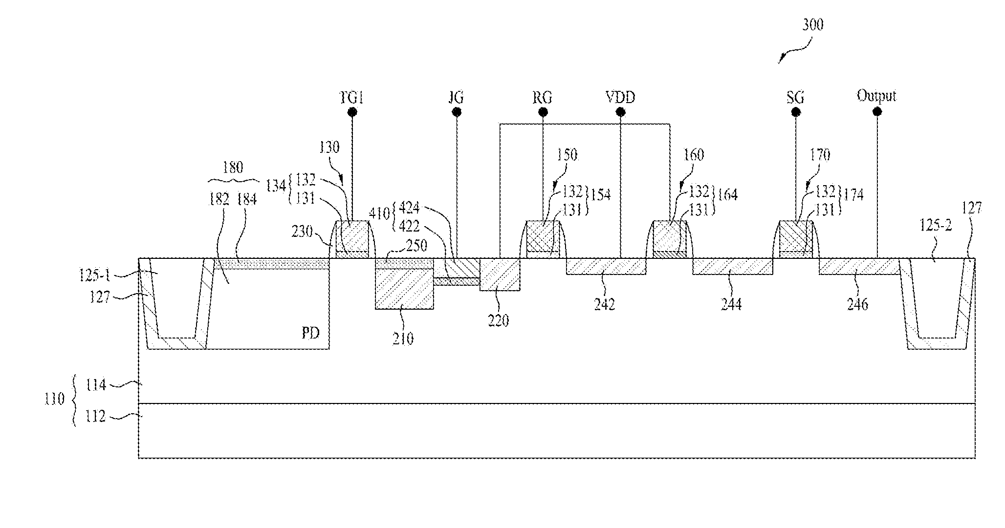
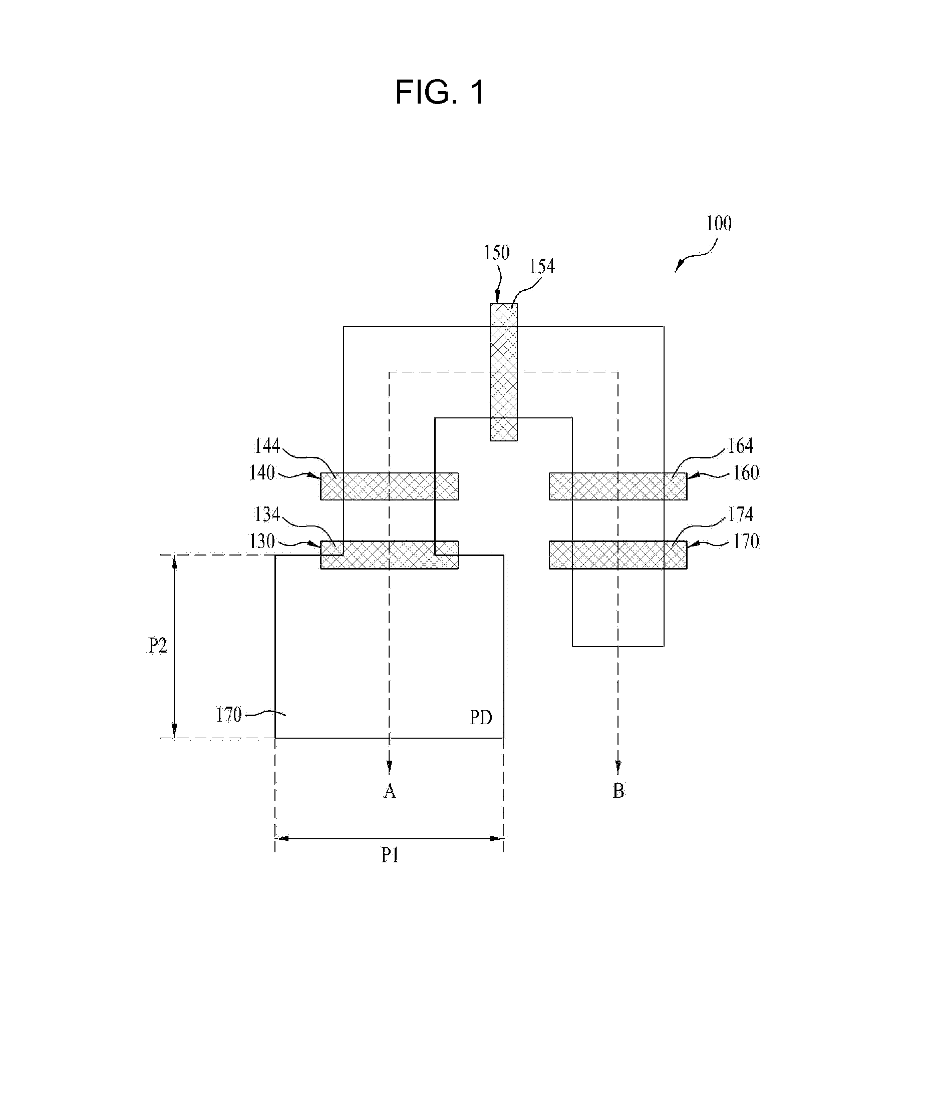
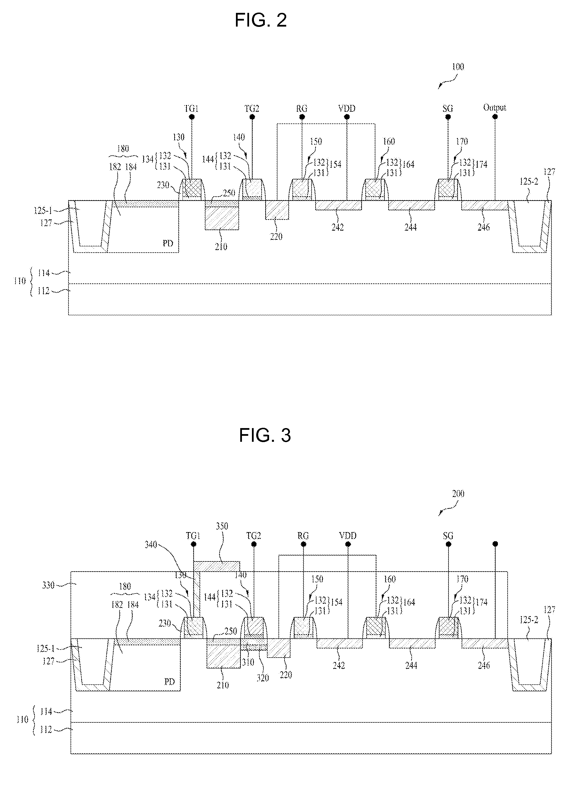
[0028]The above and other objects, features and other advantages of the present invention will be more clearly understood from the following detailed description taken in conjunction with the accompanying drawings. Prior to the description of the embodiments, with regard to descriptions of certain embodiments according to the present invention, it will be understood that, when one element such as a layer or film, a region or a structure is referred to as being formed “on” or “under” another element such as a substrate, a layer or film, a region, a pad or a pattern, the one element may be directly formed “on” or “under” the another element, or be indirectly formed “on” or “under” the another element via one or more intervening elements therebetween. Further, “on” or “under” each element is described based on the drawings.

[0029]In the drawings, the thicknesses or sizes of respective layers are exaggerated, omitted or schematically illustrated for convenience and clarity of description...


PUM


Abstract

Disclosed is an image sensor including a photodiode region on a first conductive type semiconductor substrate; a first floating diffusion region having a second conductive type, separate from the photodiode region; a second floating diffusion region having the second conductive type, separate from the first floating diffusion region; a first gate on the semiconductor substrate between the photodiode region and the first floating diffusion region; and a second gate on the semiconductor substrate between the first floating diffusion region and the second floating diffusion region, wherein the semiconductor substrate and the first floating diffusion region forms a junction area that is larger than that of the semiconductor substrate and the second floating diffusion region.

Description

[0001]This application claims the benefit of Korean Patent Application No. 10-2012-0121945, filed on Oct. 31, 2012, which is incorporated herein by reference as if fully set forth herein.BACKGROUND OF THE INVENTION[0002]1. Field of the Invention[0003]The present invention relates to an image sensor and more particularly a wide dynamic range (WDR) image sensor.[0004]2. Discussion of the Related Art[0005]An image sensor is a semiconductor device which converts an optical image into an electric signal. Representative image sensors include charged coupled device (CCD) image sensors and complementary metal oxide semiconductor (CMOS) image sensors.[0006]In general, a CMOS image sensor is classified into 3T, 4T and 5T-types depending on the number of transistors constituting a unit pixel. The unit pixel includes one photodiode and at least one transistor (for example, a transfer transistor, a reset transistor, a select transistor and / or a drive transistor).[0007]The image sensor is not cap...

Claims


Application Information

Patent Timeline
Patent Type & Authority Applications(United States)
IPC IPC(8): H01L27/146
CPCH01L27/14643H01L27/14614H01L27/146
Inventor LEE, JU ILHA, MAN LYUN
Owner DONGBU HITEK CO LTD
Why Eureka
Try Eureka