Semiconductor module

a technology of semiconductor modules and semiconductor components, applied in the direction of semiconductor devices, semiconductor/solid-state device details, electrical apparatus, etc., can solve the problems of hindering the enhancement of electric current, inability to appropriately dissipate heat from semiconductor modules, etc., and achieve the effect of convenient inspection

Active Publication Date: 2014-05-08
ROHM CO LTD
View PDF6 Cites 36 Cited by
  • Summary
  • Abstract
  • Description
  • Claims
  • Application Information

AI Technical Summary

Benefits of technology

[0024]According to this arrangement, bonded parts of the adjoining connection metal members to the first conductor layer or to the terminal do not easily overlap with each other, and therefore t...

Problems solved by technology

Therefore, it is impossible to appropriately dissipate heat from the s...

Method used


Image

  • Semiconductor module
  • Semiconductor module
  • Semiconductor module

Examples


first embodiment

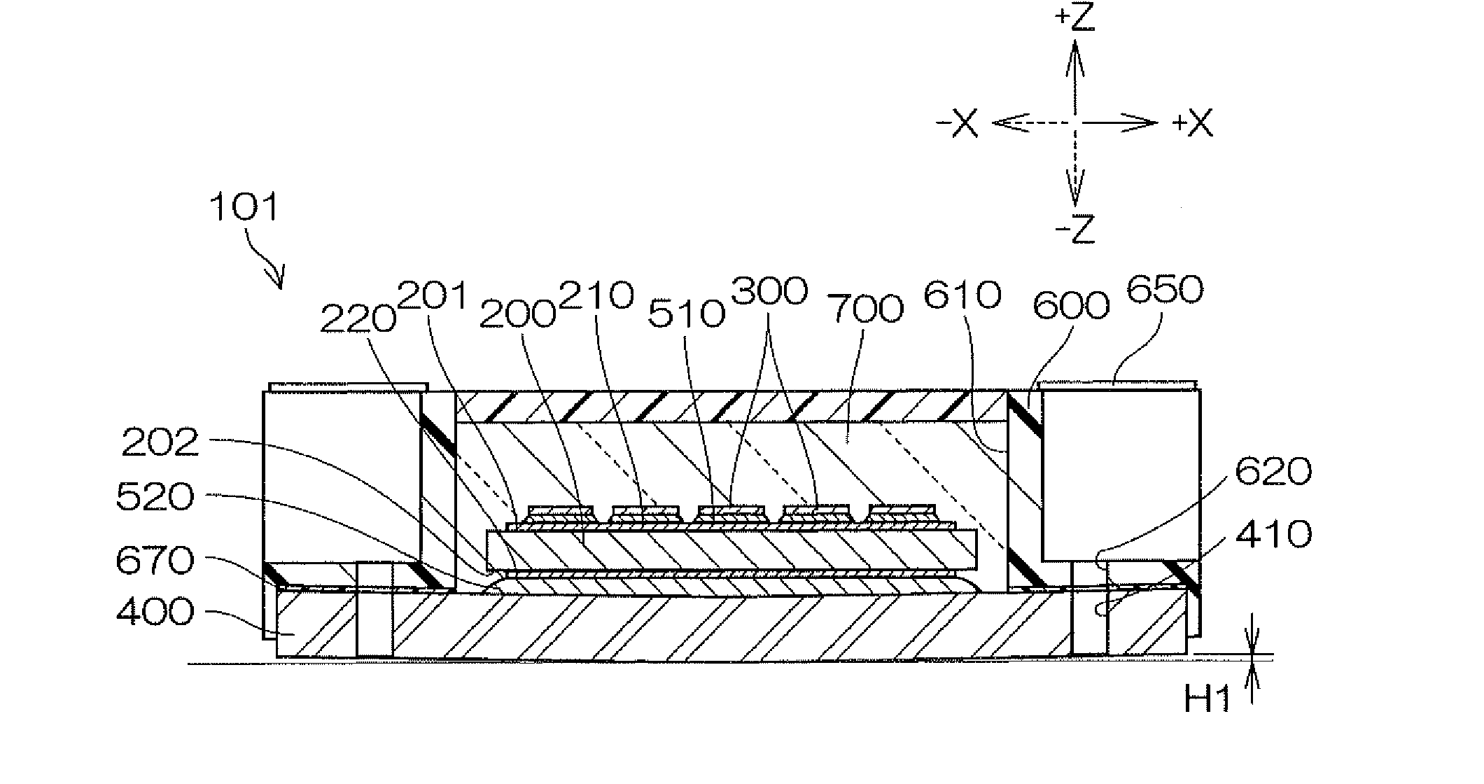
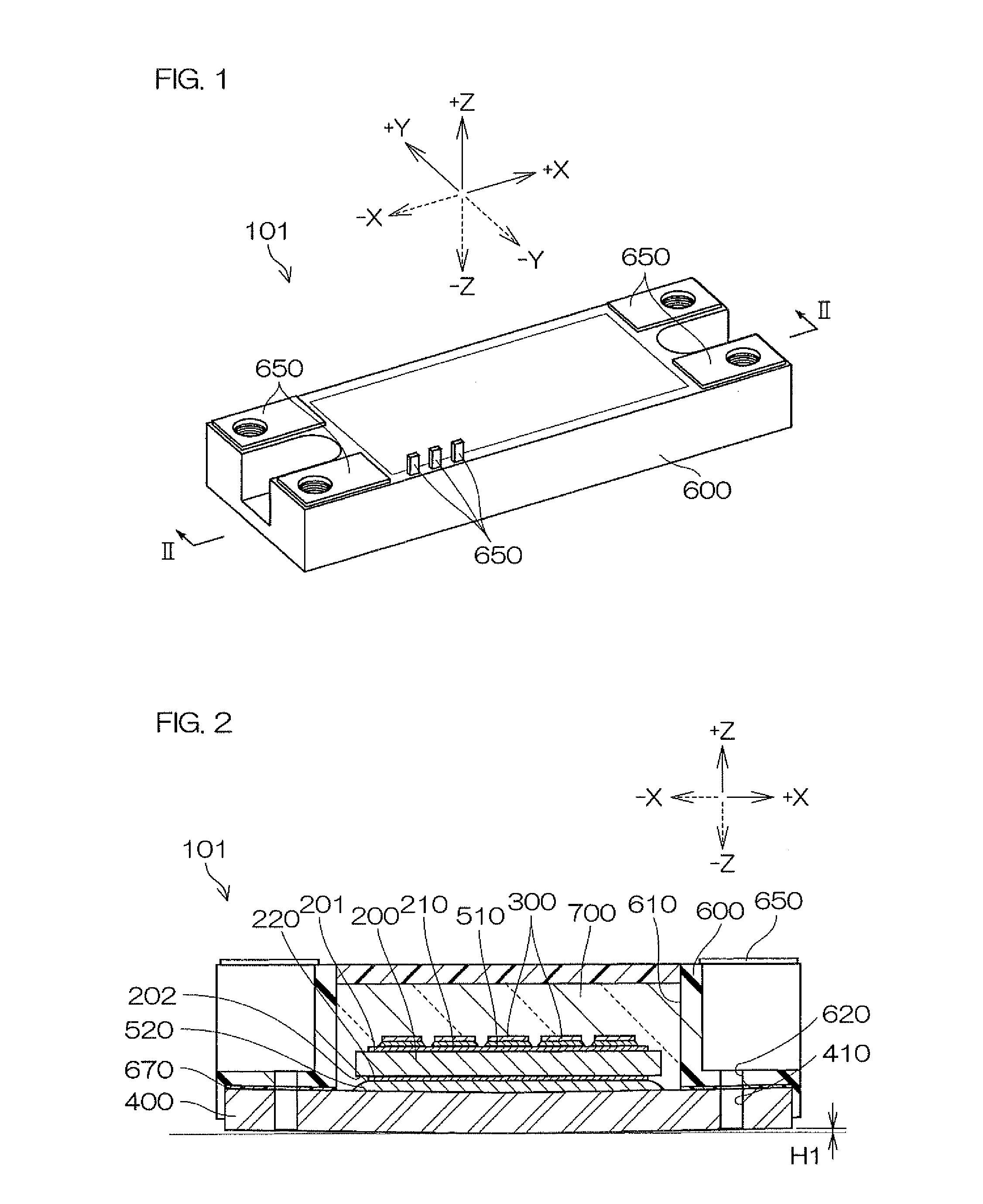
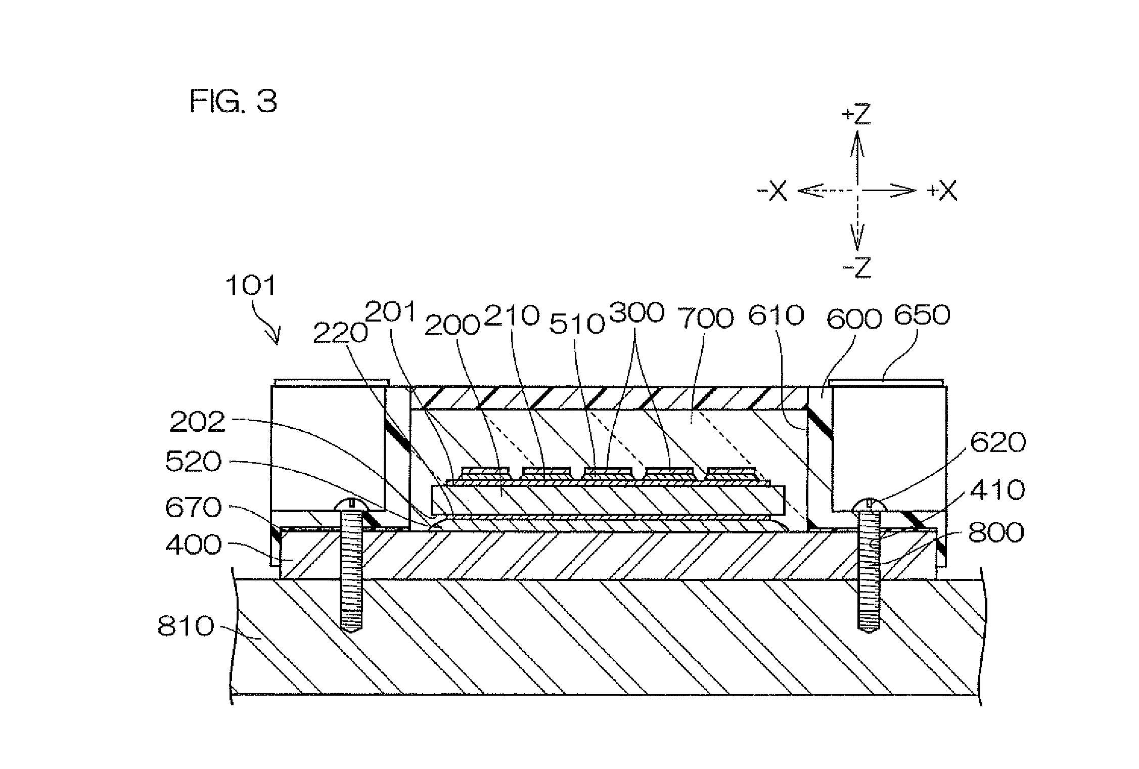
[0056]FIG. 1 and FIG. 2 show a semiconductor module according to the present invention.

[0057]The semiconductor module 101 is composed of an insulating substrate 200, a semiconductor device 300, a heat dissipation plate 400, and a case 600. Although the semiconductor module 101 is capable of realizing a high withstand voltage, a heavy electric current, and high heat dissipation ability that are suitable to be used in, for example, a high-side circuit or a low-side circuit of a power circuit that is used in trains or pieces of industrial equipment, the purpose of use of the semiconductor module 101 is not limited to this.

[0058]For descriptive convenience, in the following description, +X direction, −X direction, +Y direction, −Y direction, +Z direction, and −Z direction shown in FIG. 1 are used when necessary. +X direction and −X direction are two directions along the long side of the heat dissipation plate 400 formed in a rectangular shape when viewed planarly, and are generically re...


PUM


Abstract

A semiconductor module includes an insulating substrate (200) that is made of AlN and that has a first plane (201) and a second plane (202) both of which face mutually opposite directions, a first conductor layer (210) formed on the first plane (201), a second conductor layer (220) formed on the second plane (202), a semiconductor device (300) bonded to the first conductor layer (210) with a first solder layer (510) interposed therebetween, and a heat dissipation plate (400) that is formed in a rectangular shape when viewed planarly and that is bonded to the second conductor layer (220) with a second solder layer (520) interposed therebetween, and, in this semiconductor module, the heat dissipation plate (400) is deformed so as to become convex in a direction in which the second plane (202) is pointed when viewed from a width direction thereof.

Description

TECHNICAL FIELD[0001]The present invention relates to a semiconductor module for use in, for example, power circuits of trains or of industrial equipment.BACKGROUND ART[0002]A semiconductor module using a semiconductor device that performs a so-called switching function is used in power circuits in a wide field. In particular, a semiconductor module for use in, for example, power circuits of trains or of industrial equipment is required to have high withstand voltage, heavy electric current, and high heat dissipation ability. FIG. 28 shows one example of a conventional semiconductor module that is usable for such purposes (see Patent Literature 1, for example). The semiconductor module 900 shown in this figure has conductor layers 992 and 993 made of, for example, Cu on both sides of an insulating substrate 991 made of Al2O3. A semiconductor device 994 is bonded to the conductor layer 992 with a solder layer 995 therebetween. The semiconductor device 994 is arranged as, for example,...

Claims


Application Information

Patent Timeline
IPC IPC(8): H01L23/367
CPCH01L23/367H01L23/36H01L25/18H01L24/29H01L24/32H01L24/45H01L24/48H01L24/49H01L24/73H01L25/072H01L2224/291H01L2224/32225H01L2224/45124H01L2224/48137H01L2224/48227H01L2224/49175H01L2224/73265H01L2924/10272H01L2924/12032H01L2924/12036H01L2924/13055H01L2924/13091H01L2924/19107H01L2924/30107H01L2924/01013H01L2924/01028H01L2924/01029H01L2224/49111H01L23/24H01L23/3735H01L2924/1306H01L2924/1305H01L2224/48139H01L2924/181H01L2924/12041H01L2224/49113H01L2224/0603H01L2924/014H01L2924/00012H01L2924/00H01L2924/00014H01L23/4006
Inventor HAYASHI, KENJIHAYASHIGUCHI, MASASHI
Owner ROHM CO LTD
Why Eureka
Try Eureka