

Method of manufacturing semiconductor device
a manufacturing method and semiconductor technology, applied in the direction of semiconductor devices, basic electric elements, electrical appliances, etc., can solve the problems of difficult to form fine features by wet etching, the inability to so as to reduce the width of the electrode of the semiconductor device and reduce the damage to the surface of the semiconductor layer
- Summary
- Abstract
- Description
- Claims
- Application Information
AI Technical Summary
Benefits of technology
Problems solved by technology
Method used
Image

Examples
first embodiment
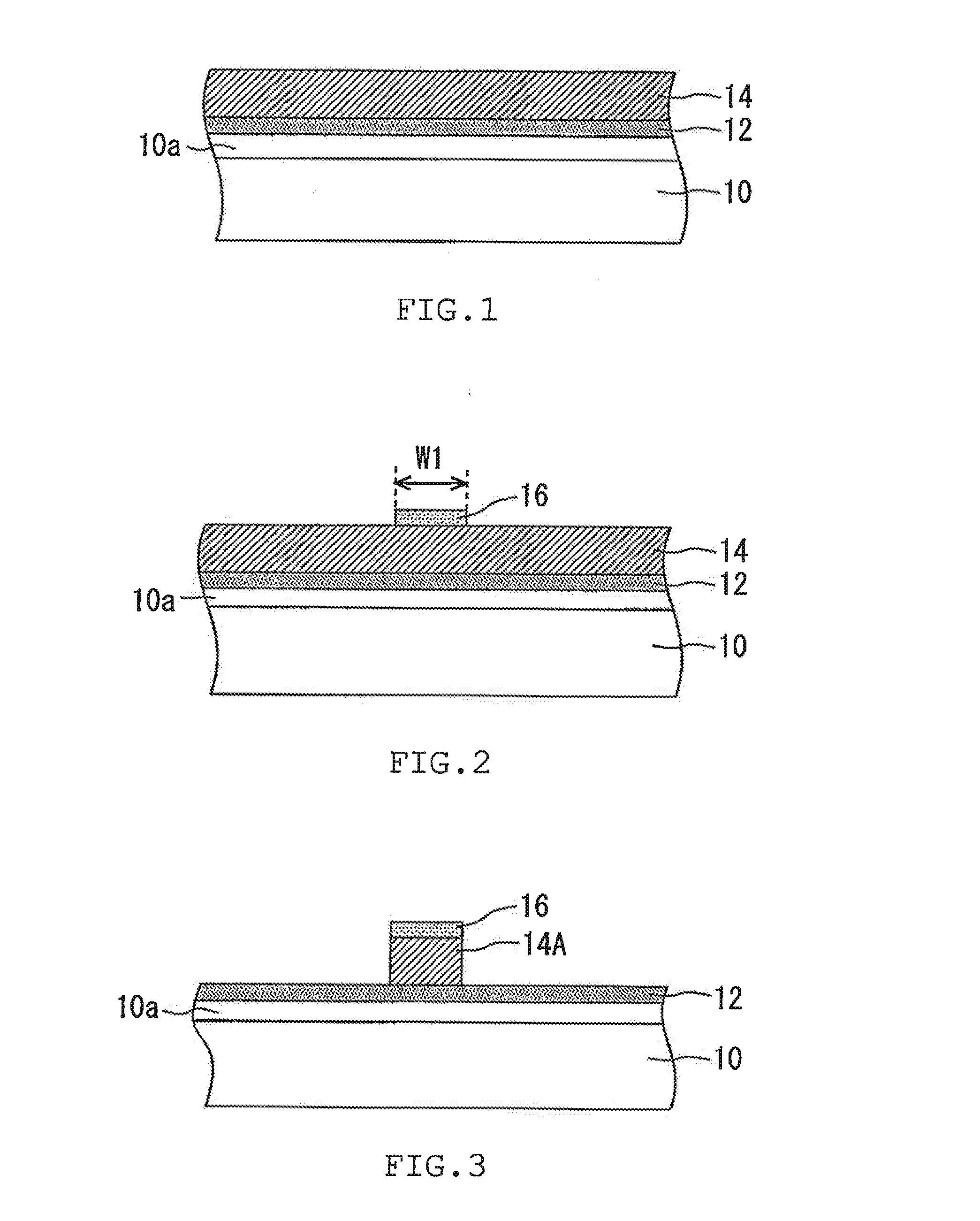
[0032]A method of manufacturing a semiconductor device in accordance with a first embodiment of the present invention will be described with reference to the accompanying drawings. The method begins by forming insulating films on a semiconductor layer. FIG. 1 is a cross-sectional view showing a first layer 12 and a second layer 14 of insulating film formed on a substrate 10. The substrate 10 is formed of, e.g., SiC, and has a semiconductor layer 10a of, e.g., GaN or AlGaN epitaxially grown on its top surface. The first layer 12 is formed of SiO disposed on the semiconductor layer 10a. The second layer 14 is formed of SiN disposed on the first layer 12.
[0033]Next, a patterned mask 16 is formed on the second layer 14. FIG. 2 is a cross-sectional view showing the mask 16 after it has been formed. This mask 16 is a resist mask or metal mask and has a width W1.
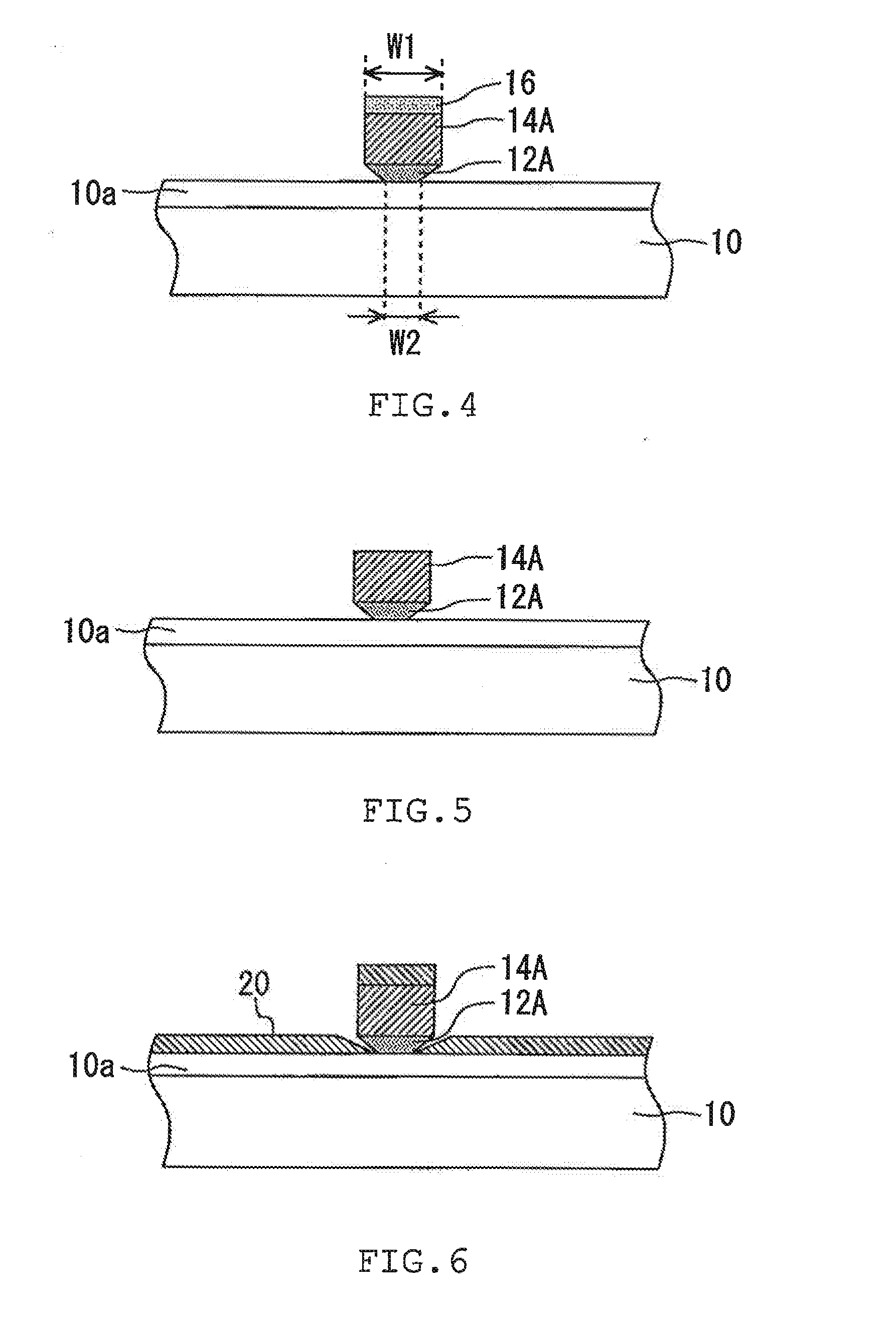
[0034]The portions of the second layer 14 that are not covered by the mask 16 are then etched away. FIG. 3 is a cross-sectional v...
second embodiment
[0046]A method of manufacturing a semiconductor device in accordance with a second embodiment of the present invention will be described with reference to the accompanying drawings. The method begins by forming a Si oxide 50 on a semiconductor layer 10a. FIG. 10 is a cross-sectional view showing the Si oxide 50 after it has been formed. Specifically, this Si oxide 50 is SiO.
[0047]Next, a patterned mask 52 is formed on the Si oxide 50. FIG. 11 is a cross-sectional view showing the patterned mask 52 after it has been formed. This mask 52 has an opening having a width W3.
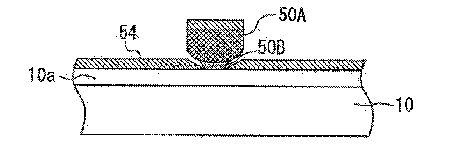
[0048]Ashing treatment is then applied to the Si oxide 50. FIG. 12 is a cross-sectional view showing the Si oxide 50 after it has been subjected to the ashing treatment. Specifically, in this step, ashing treatment is applied to the portion of the Si oxide 50 exposed through the opening of the mask 52. Ashing treatment is a treatment in which an object to be treated is oxidized, or ashed. As a result of the ashing trea...
PUM
 Abstract
Description
Claims
Application Information