Circuit stack structure

a stack structure and circuit technology, applied in printed circuit aspects, non-metallic protective coating applications, metallic pattern materials, etc., can solve the problems of increasing the manufacture or maintenance cost, increasing the risk of conductor layer damage, and affecting the quality of circuits, so as to protect the wiring from the risk of scratching, improve the qualified rate, and reduce the effect of resistan

Active Publication Date: 2014-05-22
HANNSTAR DISPLAY CORPORATION
View PDF7 Cites 10 Cited by
  • Summary
  • Abstract
  • Description
  • Claims
  • Application Information

AI Technical Summary

Benefits of technology

[0014]Since multiple through openings are formed on the fourth insulation layer, the formed second metal wires and the top surface of the protective layer all have uneven surfaces corresponding to these through openings. Therefore the differences in contact area between the convex portion and the concave portion in the foregoing known structure are reduced and the contact area of the protective layer scratched by a hard object is also reduced, so as to protect the wiring from the risk of scratch and improve the qualified rate. Furthermore, since each of the second metal wires is electric

Problems solved by technology

However, since the transition line area 60 has no scratch-proof design, damage by scratching on the transition line area 60 is often happened.
As such, the wiring of the

Method used


Image

  • Circuit stack structure
  • Circuit stack structure
  • Circuit stack structure

Examples


first embodiment

[0043]Referring to FIGS. 3 and 4, in the first embodiment, the first insulation layer 610 is disposed on the glass substrate 110, for example directly disposed on the glass substrate 110. The first conductor layer 400 is disposed on the first insulation layer 610. In other words, the first insulation layer 610 is disposed between the first conductor layer 400 and the glass substrate 110, or even the first insulation layer 610 is directly positioned between the first conductor layer 400 and the glass substrate 110.

[0044]The first propping portions 700 are disposed in the first conductor layer 400 and are coplanar with the first metal wires 410. That is, the minimum vertical distance D1 from bottom surfaces of the first propping portions 700 to a reference surface (e.g. the top surface of the glass substrate 110) is equal to a minimum vertical distance D2 from bottom surfaces of the first metal wires 410 to the reference surface (e.g. the top surface of the glass substrate 110).

[0045]...

second embodiment

[0056]In a variation of the second embodiment, when the second insulation layer 620 covers the first propping portions 700 in the second areas B, the second insulation layer 620 directly contacts the glass substrate 110 at two opposite sides of the first propping portion 700, so as to avoid physical contact between the first propping portions 700 and the first metal wires 411 disposed at two sides thereof.

[0057]Therefore, during manufacturing, the first conductor layer 401 (the first metal wires 411 and the first propping portions 700), the second insulation layer 620 and the protective layer 801 are sequentially formed on the glass substrate 110. Based on the first metal wires 411 and the first propping portions 700, corresponding convex portions are respectively formed on top surfaces of the formed second insulation layer 620 and protective layer 801 in the first areas A and the second areas B, so as to ensure that the top surface of the protective layer 801 in the first areas A i...

fourth embodiment

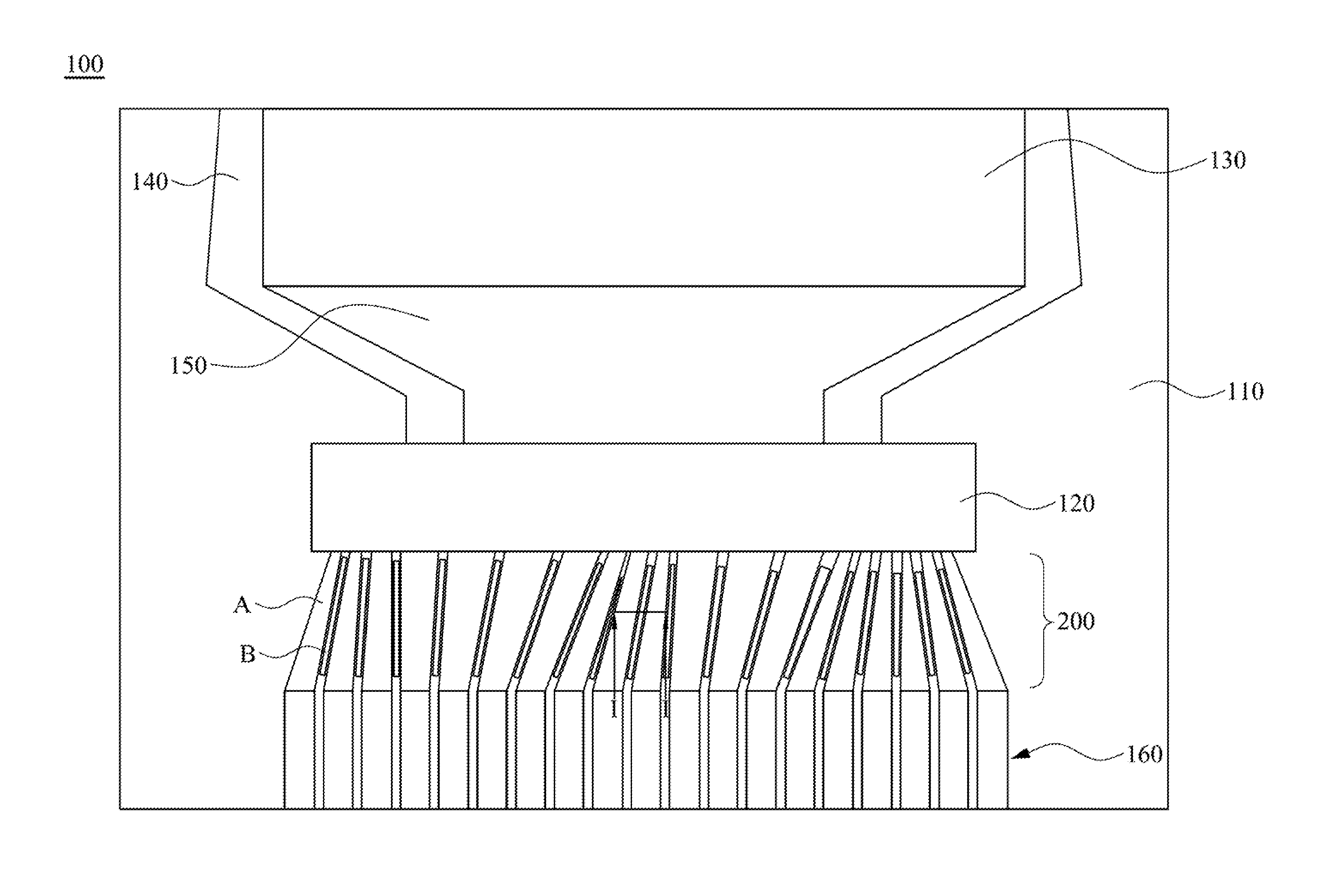
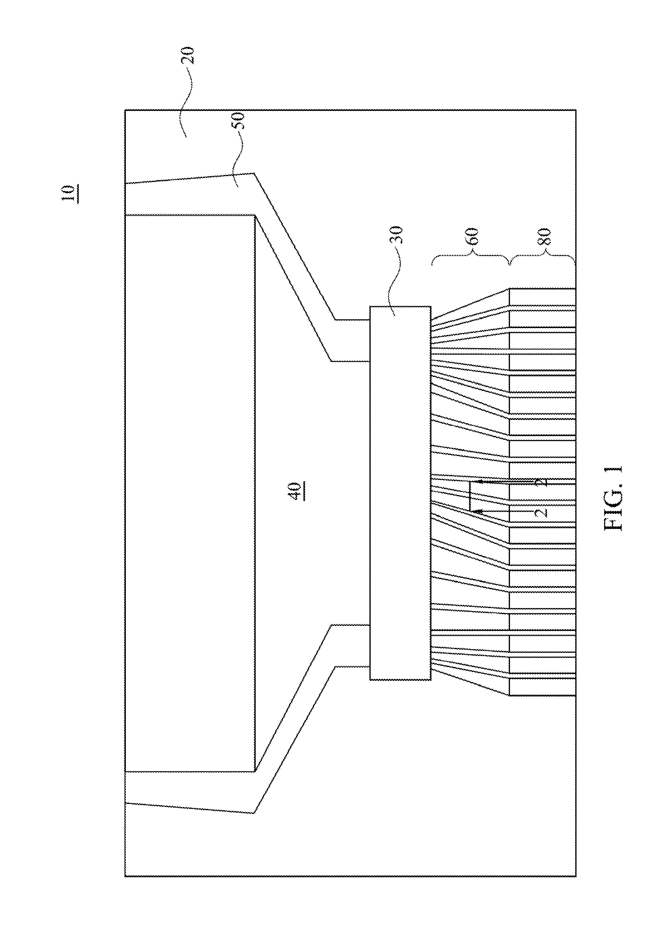
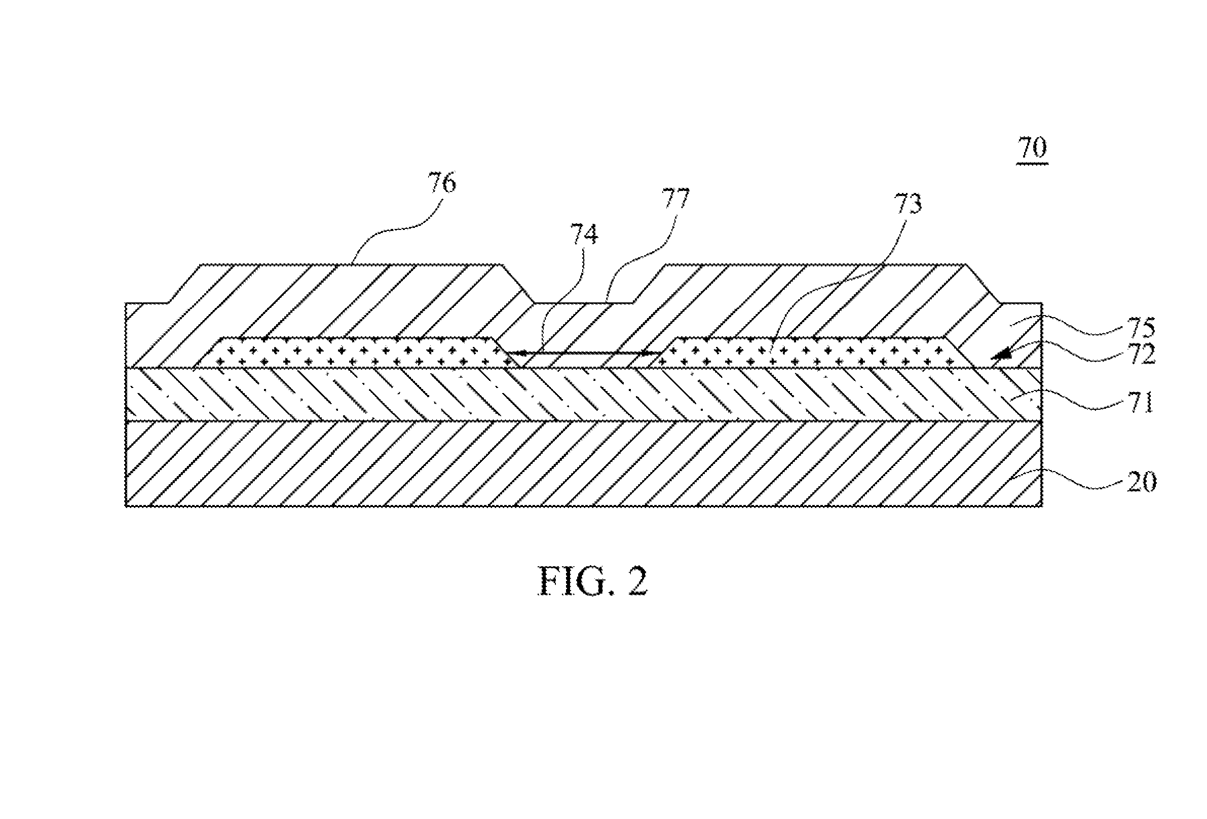
[0086]FIG. 15 is a cross-sectional view of FIG. 14 along a line Referring to FIGS. 14 and 15, The transition line area 201 includes a circuit stack structure 301. The circuit stack structure 301 includes a first conductor layer 403, a third insulation layer 630, multiple sixth propping portions 760 and a protective layer 803. The first conductor layer 403 and the third insulation layer 630 are both disposed on the glass substrate 111. The first conductor layer 403 includes multiple first metal wires 413 arranged at intervals.

[0087]A first gap G1 is disposed between any two adjacent first metal wires 413, and two ends of each of the first metal wires 413 are respectively connected to the FPC pad area 161 and the driver chip 121 (FIG. 14). The sixth propping portions 760 having long and narrow shapes are arranged in parral with each other on the third insulation layer 630, and are electrically isolated with the first metal wires 413, the FPC pad area 161 and the driver chip 121. The p...


PUM


Abstract

A circuit stack structure is provided. The circuit stack structure includes a conductor layer having metal wires arranged at intervals, propping portions respectively disposed in a gap between any two of the neighboring metal wires, and a protective layer covering the metal wires and the propping portions. The propping portions are electrically isolated with the metal wires. With supporting by the propping portions, all regions of a top surface of the protective layer corresponding to one of the propping portions are coplanar with all regions of the top surface of the protective layer corresponding to each of the metal wires.

Description

RELATED APPLICATIONS[0001]This application claims priority to Chinese application no. 201210477163.X filed Nov. 21, 2012, the entirety of which is incorporated herein by reference.BACKGROUND[0002]1. Field of Invention[0003]The invention relates to a circuit stack structure. More particularly, the invention relates to a circuit stack structure of a circuit stack structure of an active component array substrate.[0004]2. Description of Related Art[0005]FIG. 1 is a partially top view of a known active component array substrate 10. As shown in FIG. 1, the active component array substrate 10 includes a glass substrate 20, a driver chip 30, a plurality of data lines 40 and a plurality of scan lines 50. The data lines 40, the scan lines 50 and the driver chip 30 are all disposed on the glass substrate 20. The driver chip 30 is coupled to the data lines 40 and the scan lines 50, also, the driver chip 30 is connected to a flexible printed circuit (FPC) pad area 80 through a transition line ar...

Claims


Application Information

Patent Timeline
IPC IPC(8): H05K1/02
CPCH05K1/0298H05K1/11H05K1/0306H05K1/189H05K3/28H05K2201/09227
Inventor CHEN, YUNG-FUWU, RONG-BINGCHEN, PO-HSIAOWU, CHIEN-HAO
Owner HANNSTAR DISPLAY CORPORATION
Why Eureka
Try Eureka