Semiconductor device

Active Publication Date: 2014-06-12
FUJI ELECTRIC CO LTD
View PDF6 Cites 6 Cited by
  • Summary
  • Abstract
  • Description
  • Claims
  • Application Information

AI Technical Summary

Benefits of technology

This patent text describes how to improve the design of semiconductor devices to prevent a decrease in breakdown voltage and improve a turn-off breakdown voltage. This is achieved by creating a gap between the two parts of the device, which reduces the concentration of electric field at the bottom of the trench gate and prevents it from affecting the p-type extension region when the device is turned off. Overall, this design helps to enhance the reliability and performance of semiconductor devices.

Problems solved by technology

As a result, the electric field is likely to concentrate on the bottom of the termination trench and avalanche breakdown occurs at a low voltage, which results in a reduction in the breakdown voltage.
As a result, for example, the on voltage and turn-off loss increase.
Therefore, there is a concern that the electric field will concentrate on the connection portion and breakdown will occur due to current concentration.
Thus, as described above, there exists certain problems in the related art

Method used


Image

  • Semiconductor device
  • Semiconductor device
  • Semiconductor device

Examples


Embodiment Construction

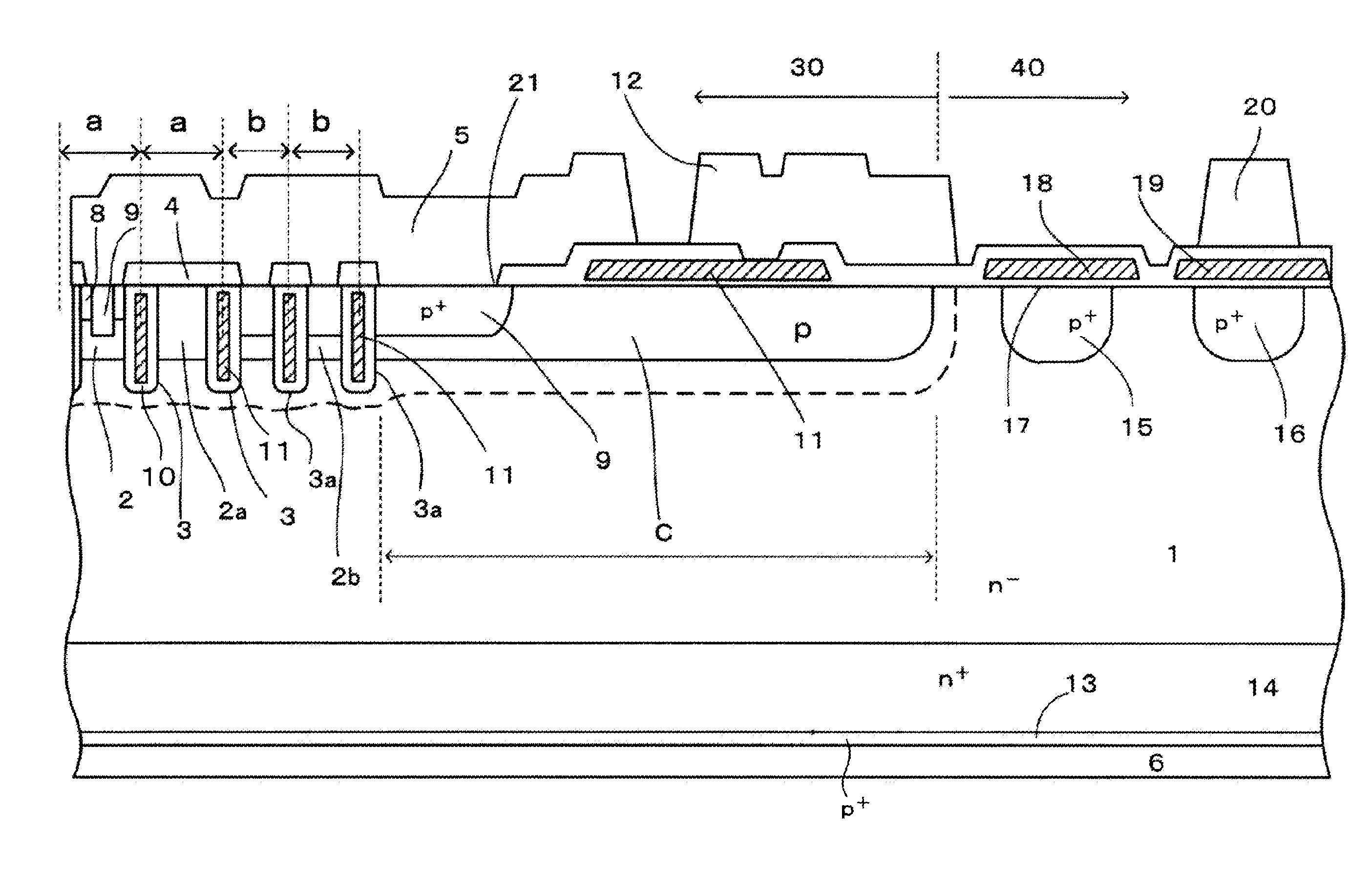
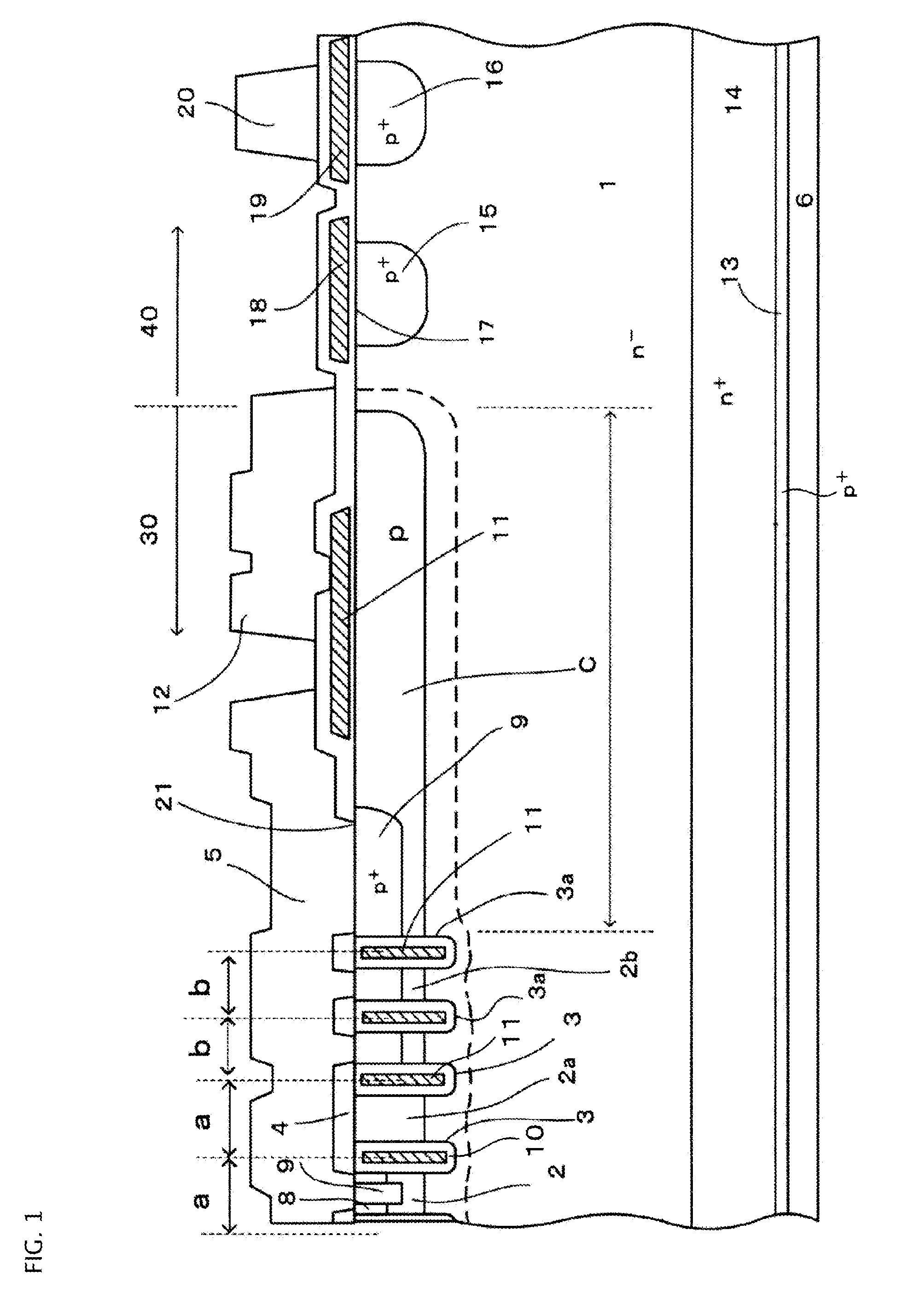
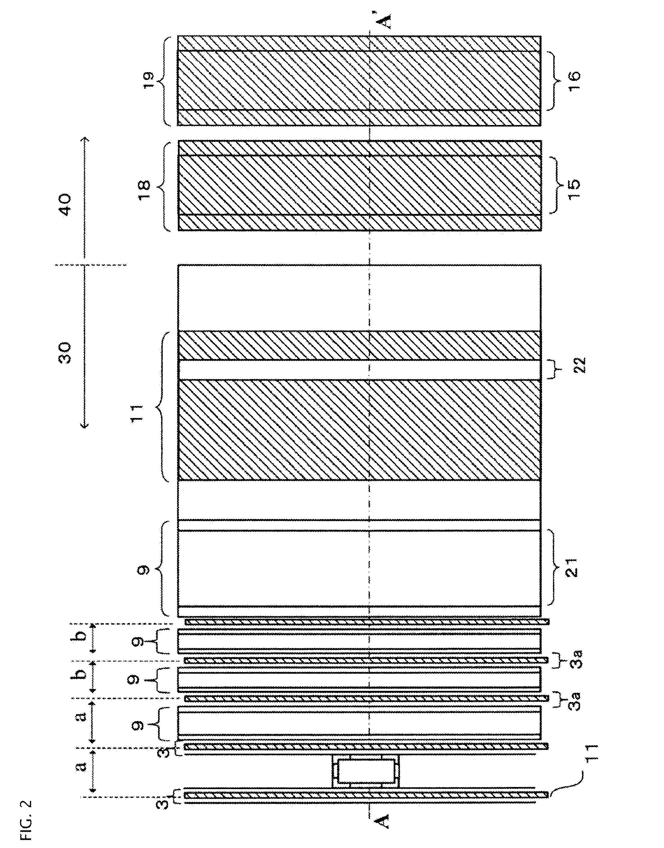
[0033]Hereinafter, a semiconductor device according to an exemplary embodiment of the invention will be described in detail with reference to the accompanying drawings. In the specification and the accompanying drawings, in the layers or regions having “n” or “p” appended thereto, an electron or a hole means a major carrier. In addition, symbols “+” and “−” added to n or p mean that impurity concentration is higher and lower than that of the layer or the region without the symbols. In the description of the following embodiment and the accompanying drawings, the same components are denoted by the same reference numerals, and the description thereof will not be repeated. In addition, various modifications and changes of the invention can be made without departing from the scope of the invention. The invention is not limited to the following embodiment.

Non-Limiting Exemplary Embodiment

[0034]The structure of a semiconductor device according to an embodiment will be described with refer...


PUM


Abstract

Some aspects of the invention include a trench gate structure including a p base layer, an n+ emitter region, a trench, a gate oxide film, and a doped polysilicon gate electrode is provided in an active region. A p-type extension region formed by extending the p base layer to an edge termination structure region can be provided in the circumference of a plurality of trenches. One or more annular outer trenches which are formed at the same time as the plurality of trenches are provided in the p-type extension region. The annular outer trenches can surround all of the trenches. A second gap between the annular outer trench and the outermost trench or between adjacent annular outer trenches is less than a first gap between adjacent trenches.

Description

CROSS-REFERENCE TO RELATED APPLICATION[0001]This application is a continuation of International Application No. PCT / JP2012 / 72823, filed on Sep. 6, 2012, which is based on and claims priority to Japanese Patent Application No. JP 2011-195970, filed on Sep. 8, 2011. The disclosure of the Japanese priority application and the PCT application in their entirety, including the drawings, claims, and the specification thereof, are incorporated herein by reference.BACKGROUND[0002]1. Field of the Invention[0003]Embodiments of the invention relate to power semiconductor devices that include a trench gates.[0004]2. Related Art[0005]With a reduction in the power consumption of a power conversion device, it is expected that the power consumption of a power semiconductor device (switching device) which plays a central role in the power conversion device will be reduced. In recent years, a power insulated gate (MOS) semiconductor device with a trench gate structure capable of considerably increasin...

Claims


Application Information

Patent Timeline
IPC IPC(8): H01L29/739
CPCH01L29/0615H01L29/0619H01L29/404H01L29/7397H01L29/0696H01L29/407H01L29/42368
Inventor KURATA, NAOKOMOMOTA, SEIJIABE, HITOSHI
Owner FUJI ELECTRIC CO LTD
Why Eureka
Try Eureka